
Testbourne Ltd
SuperVac® Materials Division:
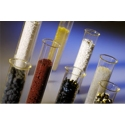
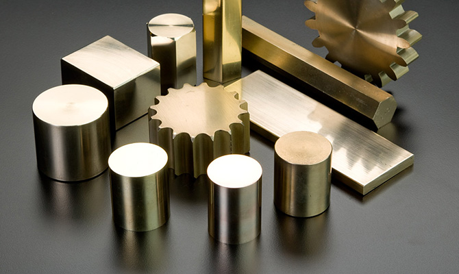
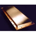
Testbourne Ltd has been supplying high purity metals, alloys & compounds to industries such as Semiconductors, Thin-films, Electronics, Electro-optics and research establishments for over 30 years. Testbourne is committed to provide the best possible service and technical expertise across a wide market area to be your first, if not single choice for an extensive selection of Metals, Alloys, Intermetallics, Compounds and Ceramics available in fabricated forms including sputtering targets, evaporation materials, powders, wire, rods & sheets. We also accommodate any custom requirements you may have.
We are proud to announce a new range of Rotatable Sputtering targets for Photovoltaic and Glass Industry.
Instrument Division:
Testbourne Limited is the representative for some of the world's leading scientific instrument manufacturers that include monitors, controllers and sensor crystals for QCM and Thin Film Technology, Sample Preparation Equipment, Thermal and E-beam Evaporation Sources, Microwave and Radio Frequency Systems, UHV feedthroughs, connectors, coaxials and viewports.
-
Exploring the Spheres of Innovation: Industries Transformed by Testbourne
14 November 2023In a world full of advanced technology and innovation, Testbourne stands as a formidable force, catering to a wide range of industries and applications with its exceptional range of products.
From scientific research to industrial processes, Testbourne’s products play a crucial role in driving progress across multiple sectors. Testbourne’s materials have revolutionised everything from medical diagnostics to renewable energy resources, empowering and driving industry innovation forward. In this blog, we look at the various industries Testbourne collaborates with and the applications our products feature in, highlighting some of the key products that power each field.
Scientific Materials for the Architectural Glass Industry
In the architectural glass industry, Testbourne takes on a pivotal role by supplying a range of specialised products that elevate the design and functionality of architectural glass, automotive glass, photovoltaics, mirrors and other coatings.
Testbourne is a worldwide supplier of sputtering targets for this industry; used for high-quality glass coatings, innovative glazing materials and cutting-edge interlayer technologies. These materials enable manufacturers to push the boundaries of creativity while meeting stringent performance requirements, resulting in glass facades that offer enhanced thermal insulation and solar control.
Scientific Materials for the Hard-Wearing and Decorative Coatings Industry
For the hard-wearing and decorative coatings industry, Testbourne provides a spectrum of specialised products that underpin both durability and aesthetics.
The materials Testbourne supplies, including sputtering targets and Arc cathodes, enhance the resistance to wear, corrosion and environmental stresses, making them ideal for the demands of industries like automotive and architecture. These materials seamlessly fuse functionality and style, ensuring that surfaces not only withstand the rigours of daily use but also exude an enduring visual appeal.
Scientific Materials for the UHV Industry
Testbourne supplies components into a variety of vacuum applications, including synchrotrons, semiconductor processing, thin film coating, spectroscopy, ion beam, x-ray, nuclear energy and MRI to the UHV industry.
CeramTec materials, like Ceramaseal UHV ceramic-to-metal feed-throughs, are ideal for all applications that require vacuum tightness and electrical insulation. Ceramic-to-metal feed-throughs not only offer freedom from leaks in vacuum environments but are resistant to high temperatures, high pressure and aggressive chemicals, making them perfect to use for UHV technology.
Scientific Materials for the Optics Industry
Optical coatings are typically found in everyday items from sunglasses and mirrors to industrial machinery like laser technology. This industry relies on precision and quality, and Testbourne delivers just that.
Our evaporation materials are used in PVH (Physical Vapour Deposition) to allow researchers, engineers and medical professionals to achieve exceptional results, pushing the boundaries of what is possible in the optics field. This range of materials is the building block for cutting-edge optical systems, used to create high-performance lenses and mirrors all the way to prisms and filters.
Scientific Materials for the Solar Industry
With the demand for renewable energy resources becoming more important, there has been considerable growth in the solar and photovoltaic industries. The efficiency of solar materials must be maintained, so sourcing high-quality materials is essential.
Testbourne’s high-grade materials, such as Inficon QCM and Guardian Controllers, improve the efficiency of solar systems. As PVD coatings become more advanced, Testbourne’s role as a high-quality material supplier becomes ideal where reflective and anti-reflective coatings are required.
Scientific Materials for the Electronics Industry
The world of electronics is an ever-evolving market, with Testbourne products being used in the production process for thin-film technology, the production of capacitors and micro-resistors.
Testbourne stands as an unwavering force in the electronics industry, providing materials and technology for a range of applications. Our diverse range of materials, from high-purity materials to electron beam gun crucibles are ideally suited to today’s technologically advanced environment.
Scientific Materials for the Medical Industry
In the dynamic ever-changing sector of the medical industry, Testbourne emerges as a vital partner, supplying a range of specialised materials that underpin critical healthcare technologies.
A flagship product is single crystals, engineered to convert forms of radiation into visible light. These Testbourne products play a pivotal role in accurate medical imaging, from PET scanners to gamma cameras, enabling precise diagnoses. With these high-quality products, testing is made simpler and more reliable.
Testbourne’s Impact Across Diverse Industries
In the vast landscape of innovation, Testbourne stands as a beacon of advancement, touching a multitude of industries and applications with its cutting-edge products. Spanning from the frontiers of scientific research to the critical infrastructure of medical technology and electronics, they play a pivotal role in the pursuit of evolution.
Are you unsure whether Testbourne has the right materials for your industry? We offer a broad range of scientific materials and instruments with bespoke customisable options. Get in touch with our dedicated team to discuss your specific requirements.
-
Unveiling Excellence: RD Mathis Components from Testbourne
14 November 2023In the realm of scientific instrumentation, precision and reliability are paramount. RD Mathis components have been at the forefront of providing premium equipment to the scientific community for decades. With an unwavering commitment to quality, innovation and customer satisfaction, RD Mathis components have a well-deserved reputation as a trusted partner for scientists, engineers and researchers around the globe.
RD Mathis Products from Testbourne
Testbourne is a trusted provider for all RD Mathis components , from evaporation boats, boxes and baskets to filaments, crucibles and liners. We offer an extensive range of sources and materials to that can fulfil your evaporation needs.
Filaments: The Spark of Excellence
Filaments by RD Mathis are the heartbeat of any evaporation process. RD Mathis boasts a comprehensive range of filaments designed to meet the diverse demands of thin film deposition. From standard tungsten filaments to exotic materials like rhenium, Testbourne offers a spectrum of RD Mathis filament options for every application. These filaments are meticulously crafted to ensure uniform and reliable evaporation, making them a cornerstone in the thin film industry.
Baskets and Heaters: Precision in Every Layer
Achieving uniform and consistent film thickness requires specialised tools. RD Mathis’ baskets and heaters are engineered with precision to facilitate even evaporation across the substrate. Whether it’s a tungsten or tantalum basket, or a versatile electron beam heater, these instruments are designed to optimise deposition processes, ensuring exceptional results with every layer.
Crucibles: The Crucial Containment
When it comes to high-temperature evaporation, choosing the right crucible is imperative. RD Mathis offers an array of crucibles crafted from refractory metals like tungsten, tantalum and molybdenum. These crucibles are built to withstand extreme temperatures, ensuring reliable containment of the materials to be evaporated. With RD Mathis crucible from Testbourne, researchers can confidently tackle complex thin film deposition challenges.
Boat Sources: Navigating Precision
Boat sources are invaluable tools for depositing a wide range of materials, particularly in e-beam evaporation applications. RD Mathis has perfected the art of boat source design, offering a diverse selection of materials and configurations. From standard tungsten boats to custom-shaped tantalum boats or molybdenum boats, RD Mathis products from Testbourne ensure that researchers have the precise tools needed to navigate the complexities of thin film deposition.
Box Sources: The Power of Encapsulation
In some applications, encapsulation is crucial to ensure the integrity of the material during the evaporation process. RD Mathis excels in providing high-quality box sources, designed to effectively contain and evaporate materials while minimising contamination. With options like tantalum and silicon monoxide box sources, RD Mathis offers a robust selection to meet the unique requirements of each deposition process.
A Legacy of Excellence
RD Mathis components provided by Testbourne stand as a beacon of excellence in the field of thin film deposition. Through their meticulously crafted filaments, precise basked and heaters, robust crucibles, versatile boat sources, and reliable box sources, they empower researchers to achieve exceptional results in their thin film endeavours. With RD Mathis as a partner with Testbourne, the future of thin film technology looks brighter than ever before.
Unsure if RD Mathis products can fulfil your requirements? Please get in touch with the Testbourne team and we can advise on the best solution from our portfolio of solutions and partners. We offer a broad range of scientific instruments and materials with bespoke options, simply let us know what you need!
-
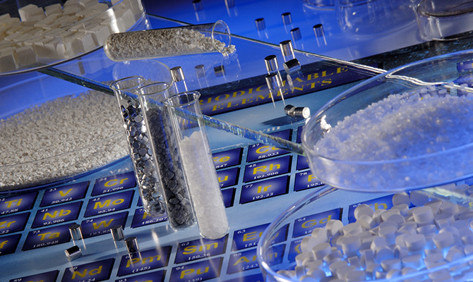
Purity Redefined with High Purity Materials, from Testbourne
27 September 2023In the realm of cutting-edge technology and scientific research, the demand for high-purity materials has reached unprecedented levels. These materials, characterised by their exceptional purity and precise compositions, play a vital role in numerous industries, including electronics, pharmaceuticals and aerospace.
Testbourne stands as an industry leader among suppliers of high purity materials, offering a diverse range of pristine substances that fuel innovation and advancement in today’s fast-paced world. In this blog, we will look at the world of high-purity materials, showcasing the diverse options from metal sheets, foils, wires and rods.
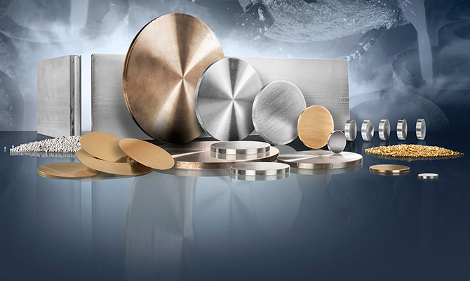
High Purity Metal Sheets
Testbourne’s high-purity metal sheets are prized for their exceptional quality and precise composition. With purities reaching up to 99.999% (5N) and beyond, these sheets are vital components used within industries like electronics and telecommunications.
The consistency and reliability of Testbourne’s metal sheets allow engineers to fabricate high-performance electronic components, thin-film devices and semiconductor substrates with unmatched precision and efficiency.
Ultra-Thin Foils for Precision ApplicationsThe ultra-thin foils, which can be as thin as a few micrometres, are vital in advanced research, medical devices and high-tech manufacturing processes. The purity and uniformity of ultra-thin metal foils make them ideal for cutting-edge fields, like nanotechnology and microelectronics, which require high precision and accuracy.
The medical sector also benefits significantly from these precision foils. When used in medical diagnostics and imaging, where precision is vital, Testbourne’s foils provide a reliable foundation for creating critical components that aid accurate diagnoses and for creating cutting-edge material equipment.
High Purity Metal Wires
In applications where robustness and electrical conductivity are paramount, high purity metal wires are a leading choice. With purities up to 99.9999% (6N) and precise diameters, Testbourne’s wires are essential in aerospace engineering and specialised instrumentation.
Metal wires significantly contribute to the advancement of specialised instrumentation in research laboratories and scientific facilities. Whether it is for high-precision sensors or state-of-the-art analytical instruments, these wires serve as the backbone, guaranteeing accurate measurements and reliable data collection.
Versatile Precision Rods
Testbourne’s high purity metal rods have a versatile use across diverse industries, leaving a profound impact on medical devices, industrial machinery and analytical instruments.
In medical devices, where biocompatibility are of paramount importance, metal rods serve as a crucial component in implants, surgical instruments and diagnostic tools. Their mechanical properties and purity ensure seamless integration into the human body.
Whereas, in the realm of industrial machinery, where precision and durability are prerequisites, these rods act as building blocks for components that withstand harsh conditions and deliver optimal performance.
Testbourne’s Exceptional Materials
Testbourne’s wide range of high-purity metal sheets, foils, wires and rods represent a testament to dedication in delivering excellence and empowering innovation across diverse industries. With purities that surpass industry standards, these materials lay the foundation for ground-breaking research and advanced technologies and enhance industrial applications.
Whether it is fabricating high-performance electronic components, pushing the boundaries of nanotechnology, transmitting electrical power efficiently, or creating life-changing medical devices, Testbourne’s high-purity materials continue to shape the future of science and technology. If you cannot find the high-purity material you need from our extensive selection, please contact the team at Testbourne, where we can advise you on the best solution and products for your applications.
-
Innovation Technology, our Partnership with INFICON
27 September 2023Testbourne partners with INFICON to provide innovative instrumentation, critical sensor technologies and advanced thin film deposition software that enhance productivity and quality. Discover more about INFICON and the products they provide.
Who is INFICON?
INFICON is a global technology company that specialises in manufacturing and providing advances solutions for a wide range of industries. With world-class manufacturing facilities in Europe, the United States and China, INFICON focus on developing solutions for applications such as leak testing, vacuum technology, thin film deposition and chemical analysis.
Products:
At Testbourne, we offer a selection of leading products by INFICON, including:
- Deposition Controllers = used to monitor or control film thickness during deposition using a QCM sensor.
- Deposition Monitors = are used similarly to deposition controllers, but simpler for applications where no rate of control is needed.
- Sensors and Sensor Feedthroughs = houses and cools quartz crystals, as well as making the electrical connection between the crystal and the feedthrough.
- Quartz Sensor Crystals = a crucial component of the control system, enabling precise and repeatable thin film deposition for a wide variety of high-value end uses.
- Accessories and Replacement Parts = we provide a selection of accessories and replacement parts for INFICON sensors, deposition controllers and monitors.
Applications
INFICON’s thin film deposition technology has a multitude of applications across different industries. Due to its durability and performance, these systems are employed in the manufacturing of optical coatings, anti-reflection coatings and mirrors.
Additionally, INFICON solutions have high thermal conductance, meaning they are utilised in the application of decorative coatings on products including jewellery, watches, eyewear and architectural elements.
Contact Us
Could INFICON technology be right for your needs? Contact the Testbourne team and we can advise you on the best solution and products for the application. At Testbourne we offer a wide range of scientific instruments and materials with custom options, simply let us know your requirements.
-
Evaporation Materials and the Evaporation Process
27 September 2023In the territory of thin film deposition techniques, evaporation stands as a versatile and precise method for creating thin films with unique properties. Central to this process are evaporation materials, which enable controlled vaporisation and deposition onto substrates.
Testbourne is a trusted supplier of evaporation materials and electron beam gun crucibles, offering a wide range of materials for diverse applications.
Materials Used for Evaporation
Evaporation materials, used for thermal evaporation and deposition processes, can be characterised by their high purity levels, and can be easily manipulated to desired film composition, properties and applications.
- Metals: Metals like gold, silver, aluminium, copper and titanium are commonly used for their excellent thermal and electrical conductivity.
- Oxides: Evaporation materials in the form of oxides offer excellent optical, electrical and mechanical properties.
- Nitrates: Popular for their hardness, thermal stability and wear resistance, nitrates find applications in decorative films and wear-resistant coatings.
Electron Beam Evaporation Process
Electron beam evaporation is a method of thin film deposition involving the use of an electron beam source. This process offers unique advantages in terms of precise control and high deposition rates.
The Process:
1. Vacuum Chamber Preparation
Similar to thermal evaporation, the process begins with the preparation of a vacuum chamber. The chamber is meticulously cleaned and evacuated to a high vacuum to create an optimal deposition environment.
2. Loading the Evaporation Source
The evaporation material, in the form of a rod or pellet, is placed in a crucible or boat made of refractory metals, such as tungsten or molybdenum as these materials can withstand the high temperatures generated by the electron beam.
3. Electron Beam Generation and Focusing
An electron beam gun generates a highly focused beam of electrons that is directed toward the evaporation source, causing the material to rapidly heat up and vaporise.
4. Film Deposition onto the Substrate
The substrate, held at a temperature-controlled stage, is carefully positioned in the path of the evaporated material. The vaporised material condenses onto the substrate, forming a thin film with precise control over thickness and uniformity.
5. Monitoring and Control
Throughout the process, parameters such as beam current, deposition rate and substrate temperature are closely monitored and adjusted to achieve the desired film properties.
Testbourne: A Leading Supplier of Evaporation Materials
Evaporation materials, coupled with the electron beam evaporation process, open up endless possibilities in thin film deposition.
At Testbourne, we have a comprehensive range of evaporation materials and expertise in the electron beam evaporation process. Our materials cater to a wide range of applications, from electronics and optics to energy for a range of industries and research. If you require any help or have any questions, contact the friendly team at Testbourne.
-
Latest Products from CeramTec
10 July 2023Discover the latest products from CeramTec, offering advanced ceramics and Ceramaseal® hermetic component solutions.
High Density Sub-Ds
Compared to a Standard Sub-D, High Density Sub-Ds have:
- Lower voltage rating: 375V DC
- Lower current rating: 2 Amps/pin
- Same temperature range: -269C to 450C
- Same pressure at 20°C: 1350 PSIG (15 Pin)
- Different pin diameter: .030" [0.76mm]
- Different pin counts: 15, 26, 44, 62, 78
Push-Pull Connectors
Some advantages of the push-pull coaxial connectors are:
- Ideal for applications which require frequent plug removal
- Very simple, safe plug connectivity and disconnecting
- Flexible design - comes in all standard flanges and weldable configurations
Sub-Cs
Sub-Cs are higher density multi-pin connectors with plugs in smaller flanges (1.33”CF), essentially providing all the capability of a Sub-D in a smaller version.
Power Boots
The new and improved power boots offer the following benefits:
- Lower lead times - this has come down from 20+ weeks to less than 6 weeks if not in stock
- Custom lengths are available
- Lower costs
Updated Mil-C-26482s
The original design for Mil-C-26482 Connectors had a single glass-ceramic perform for all pins which would produce inconsistent results when sealing. However, in the new design:
- Each pin has its own small preform which has led to very consistent results
- It's easy to plan deliveries accurately
- All ratings are identical, parts have been fully tested and perform the same if not better on all ratings
Updated Spade Type Thermocouples
The Spade style contacts and air-side thermocouple plugs that CeramTec has historically used on Thermocouples have been discontinued.
CeramTec has found a replacement manufacturer for the spade contacts and plugs, which they consider a direct replacement – the components are interchangeable.
All thermocouple feedthrough part numbers will remain the same, but the replacement plug numbers will change from 8151-XX to 25735-XX.
High Power Mil-C-5015 Connectors & Power Ds
A high powered multi-pin connector in a small footprint, this product offers:
- Standard air-side connectivity (Mil-C-5015)
- Simplified Sub-C style Vacuum side Connectivity
- Copper-cored pins for higher current carrying capabilities (up to 20 Amps)
- Glass-ceramic Seals for simplified design & high pressure capabilities
- 3, 4, 6, 10, 20 & 35 pin versions
View the full range of CeramTec products or get in touch with the Testbourne team to find out more.
-
New Product - 3D Printing Metal Powder
10 July 2023We are excited to introduce 3D printing metal powders to our vast range of scientific materials.
3D printing metal powders are the preliminary base materials for most 3D printing processes that produce metallic parts.
3D Printing Process
3D printing is the manufacturing of parts and products in a layer-by-layer fashion. Both the characteristics of the metal powder and the type of the 3D printing process determine the properties of the end product.
Portfolio of Powders
Nickel base high-temperature alloy powders like Inconel 718, Inconel 625
Cobalt alloy powder like CoCrMo, CoCrW
Titanium alloy powder like Ti6Al4V
Aluminium alloy powder like AlSi10Mg, AlSi7Mg
Iron alloy powder like SS316L, H13, 18Ni300
Stainless steel powder, CuSn10 and so on
Get in touch if you would like to find out more!
-
V2023 Vacuum Plasma Surface Coating International Conference & Exhibition
10 July 2023We are pleased to announce that Testbourne will be exhibiting at the V2023 Vacuum Plasma Surface Coating Exhibition in Dresden, Germany from 18 - 21 September 2023.
The V Conference is the meeting place for the vacuum, plasma and coating industry.
Speakers and exhibitors from industry and science will present the latest developments and innovations in the industry to the trade audience.
Meet with the European community. Discover the exhibiting companies. These leading companies offer new opportunities and innovative products to advance your projects.
The V Conference is the largest European platform for the exchange of business
At Testbourne we hope you can find some time to visit us at our booth (number (to follow) at the V2023 to discuss your material requirement for R&D or production.
Get in touch to arrange a meeting ahead of the conference.
-
PLATHINIUM - Plasma Thin Film International Union Meeting
10 July 2023We are pleased to announce that Testbourne will be exhibiting at the PLATHINIUM meeting 2023 in French Riviera from 11 - 15 September 2023.
PLATHINIUM (Plasma Thin film International Union Meeting) is now a recognized biennial meeting covering plasma physics, plasma processing and plasma applications emerged, in 2019, from combining the former conferences CIP, ITFPC and MIATEC.
The topics deal with a wide range of plasma configurations from low to atmospheric pressure using plasma excitation methods at varying frequencies and confinement by magnetic fields also. Consequently, PLATHINIUM 2023 will also focus on the applications from traditional to innovative fields such as thin films and coatings in micro and optoelectronics, automotive, aeronautics industries, and expands to nanoparticles and multifunctional nanocomposites fabrication and to emerging new fields such as plasmas, thin films and nanostructures used in environmental, energy, biomedical and agricultural applications.
At Testbourne we hope you can find some time to visit us at our booth (number 24) at the PLATHINIUM to discuss your material requirement for R&D or production.
Get in touch to arrange a meeting ahead of the conference.
-
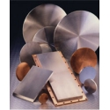
Discover Sputtering Targets from Testbourne
10 July 2023Testbourne is a leading provider of sputtering targets. Sputtering is a technology proven to be capable of depositing thin films from a variety of materials into different shapes and sizes materials. This process can be scaled up to include small research or large manufacturing processes. Discover more about the types of sputtering targets we provide and the different materials available from Testbourne.
What are Sputtering Targets?
Sputtering targets are materials that are used to create thin films in a process called sputter deposition. Sputtering targets are used to produce low-radiation coated glass, used in building construction due to its renewable energy properties, such as saving energy, saving light and for aesthetics.
The 3 Main Types of Sputtering Targets
Our sputtering targets can be produced from a wide range of materials, such as metals and compounds, using processes including rotatable target technology. The choice of material very much depends on the desired properties of the thin film, such as conductivity, renewability, or optical properties.
We offer 3 main types of sputtering targets:
1. Metal Sputtering Targets
Metal sputtering targets are made from pure metals, such as aluminium, copper, gold, silver, titanium, or metal alloys. Pure metals are most commonly used in the production of electronic devices, such as semi-conductors. Whereas metal alloys are used more commonly in the production of wear-resistant coatings for cutting tools, and biomedical or aerospace components.
At Testbourne our metal targets are offered in various purity levels to suit your specific requirements. Our manufacturing processes for metal sputtering targets depend on the properties of the target metal and its application and thus the fabrication methods we use vary from vacuum melting and rolling, to hot-pressed, vacuum hot-pressed and forged.
2. Compound Sputtering Targets
Compound sputtering targets are frequently used in industries, including semiconductors, and optical coatings.
The use of compound sputtering targets has several advantages over metal targets, including the ratio of the different elements in the film that can significantly affect its chemical, electrical and optical properties. Also, in comparison to metal sputtering targets, compound targets have a higher durability, so they are more resistant to erosion and cracking.
Testbournes' compound target production methods vary from vacuum hot pressing, hot isostatic pressing, cold isostatic pressing, and cold press sintering, depending on the required metal targets.
3. Rotatable Sputtering Targets
Rotatable sputtering targets have a cylindrical shape and are usually made up of metal or ceramic materials. The most common targets are available in chromium, tin, zinc and niobium alloys. Rotatable target technology has been highly used in large area coating manufacturing of architectural glass and flat panel displays. They get their name from the way they rotate during the sputtering process, allowing for a longer target life.
Using rotatable sputtering targets has advantages over other sputtering targets as they allow the use of higher densities because of the even spread of heat build-up over the target surface area. Additionally, they can improve the quality of deposited films, making them a popular choice in industries such as electronics, optics and semiconductors.
Our Service
Unsure if Testbourne has the right materials for you? We offer a broad range of scientific materials with bespoke options. Get in touch with our team and we can discuss your sputtering target requirements.
-
The Benefits of Target Bonding
10 July 2023Testbourne offers a complimentary target bonding service using various metallic or silver epoxy techniques, including indium-based metallic bonding, elastomer bonding, and supplying silver-based epoxy bonding kits.
What is Target Bonding?
Target bonding, in relation to sputtering targets, refers to the process of attaching the sputtering target material to the backing plate of a sputtering system. This helps to shield the sputtering targets from warping, cracking, and other damages during the sputtering process. The layer of bond creates a suitable interface to allow transfer of heat from the target surface via the backing plate which is being water cooled.
Why is Target Bonding Used?
Target bonding is used in sputtering to ensure the stability, efficiency, and longevity of the sputtering process. It is necessary to prevent the sputtering target material from vibrating or moving during the sputtering process, which could lead to uneven deposition of the material onto the substrate, leading to poor-quality films.
The bonding process can also enhance the thermal conductivity between the target material and the backing plate, allowing for higher heat dissipation during the sputtering process, and help prevent cracking. This process can also improve electrical conductivity, leading to more effective sputtering and improved film deposition.
Methods of Target Bonding
Testbourne offers two different types of target bonding, depending on the specific requirements of the sputtering process and application, as well as the properties of the sputtering target and backing plate materials.
1. Indium Bonding
Indium has very good thermal and electrical conductivity, its temperature is rated to ~150 oC.
Indium allows easier separation of the target from backing plate after use so backing plate can be reused.
2. Elastomer Bonding
Elastomer bonding is suitable for high-temperature applications as it provides good vibration-dampening and thermal expansion properties. This is an excellent alternative to Indium bond when melts during sputtering. Our elastomer is rated to 270 v. Elastomer allows more fragile targets, low melting point materials to be bonded and lowering the risk of breakages.
6 Benefits of Target Bonding
Target bonding plays a critical role in the performance and reliability of sputtering targets and there are several benefits associated with this.
1. Enhanced Target Stability
During the sputtering process, target bonding can enhance the mechanical stability of the sputtering target and prevent vibrations or movements, which could lead to inconsistent film thickness and poor film quality.
2. Improved Heat Transfer
For bonding you would use thinner sputtering targets which allows the material to transfer heat quicker to the backing plate, as well as save on costs on materials.
Effective target bonding helps in the prevention of thermal stress and cracking, which can significantly impact the product lifespan.
3. Better Electrical Conductivity
Improved electrical conductivity between the sputtering target and power supply is an additional benefit of appropriate target bonding, resulting in enhanced sputtering efficiency and superior film deposition.
4. Longer Target Lifetime
High-quality target bonding can extend the lifetime of a sputtering target, reducing the frequency of needing to replace the target and associated downtime.
Ceramics targets are prone to cracking due to thermal shock, however, when bonded the cracked sections stay attached and can continued to be used. Bonding also helps to prevent warping.
5. Consistent Film Deposition
A well-bonded sputtering target can produce a more uniform deposition rate, leading to improved film thickness control and the overall quality of the film.
6. Improved R&D Capabilities
Bonding allows larger sizes to be produced where it is technical impossible to make single section designs.
Inclusive Services
At Testbourne, our objective is to provide efficient, superior services with full technical support to all our customers. We have the facilities to cater for small volume R&D requirements through to large-scale mass production quantities, while still maintaining the highest quality product. If you have any questions about the various services and products we offer, please get in touch with our expert team and we would be happy to help.
-
Glasstec 2018 - the meeting point for the world of glass
12 December 2018Glasstec is the meeting point for the world of glass, not only the world‘s largest trade fair for the glass industry and its suppliers but also the most international event.
Discover the world of glass
Worldwide-unique: there ist no other event, which presents the entire spectrum of the material glass - from production to processing and application right up to receycling
- 1.217 exhibitors from 51 countries and around 43,000 visitors from 87 countries
- Unique global picture of the entire glass supply chain process
- Unique supporting programme consisting of special shows and congresses
- Best marks by visitors and exhibitors -
Vacuum Expo 2018 - 10th & 11th October 2018 Ricoh Arena, Coventry
12 December 2018VACUUM EXPO brings together all aspects of industry and research, helping visitors develop strong business relationships, research solutions, examine technologies for academia, research and technology for manufacturing.
PROFESSIONAL EDUCATION: Attend one, or multiple talks, or spend the whole day or days in a specific meeting - all offered free-of-charge - The Vacuum Symposium (all free except training courses).
Handle, touch and feel equipment, instruments, components and watch demonstrations.
Discover the difference: On the internet one product can seem just like another. But it is getting down to the in-depth detail face-to-face with a specialist which will enable you to make a better informed purchasing decision.
Find a new supplier: Fed up with poor communications, poor delivery, poor products? At Vacuum Expo you will be able to meet with a new supplier.
Solve: your vacuum technology, vacuum system, vacuum process problems with the numerous specialists at the event.
-
SVC TechCon 2018 - 61st Annual Technical Conference
12 December 2018SVC TechCon 2018 will be held from May 5 – May 10, 2018 at Gaylord Palms Resort and Convention Center, Orlando, Florida, USA.
TechCon participants come from all facets of the Vacuum Coating industry: manufacturers, suppliers, end users, researchers, managers, development engineers, educators and students. The program scope spans from fundamental aspects and innovative ideas all the way to manufacturing finished products.
Please come and visit us Stand 213 -
Vacuum Expo 2016 - Technology in a Vacuum
12 December 2018VACUUM EXPO brings together all aspects of industry and research, helping visitors develop strong business relationships, research solutions, examine technologies for academia, research and technology for manufacturing.
PROFESSIONAL EDUCATION: Attend one, or multiple talks, or spend the whole day or days in a specific meeting - all offered free-of-charge - The Vacuum Symposium (all free except training courses).
Handle, touch and feel equipment, instruments, components and watch demonstrations.
Discover the difference: On the internet one product can seem just like another. But it is getting down to the in-depth detail face-to-face with a specialist which will enable you to make a better informed purchasing decision.
Find a new supplier: Fed up with poor communications, poor delivery, poor products? At Vacuum Expo you will be able to meet with a new supplier.
Solve: your vacuum technology, vacuum system, vacuum process problems with the numerous specialists at the event.
-
Vacuum Expo 2017 - 11th & 12th October 2017 Ricoh Arena, Coventry
12 December 2018VACUUM EXPO brings together all aspects of industry and research, helping visitors develop strong business relationships, research solutions, examine technologies for academia, research and technology for manufacturing.
PROFESSIONAL EDUCATION: Attend one, or multiple talks, or spend the whole day or days in a specific meeting - all offered free-of-charge - The Vacuum Symposium (all free except training courses).
Handle, touch and feel equipment, instruments, components and watch demonstrations.
Discover the difference: On the internet one product can seem just like another. But it is getting down to the in-depth detail face-to-face with a specialist which will enable you to make a better informed purchasing decision.
Find a new supplier: Fed up with poor communications, poor delivery, poor products? At Vacuum Expo you will be able to meet with a new supplier.
Solve: your vacuum technology, vacuum system, vacuum process problems with the numerous specialists at the event.
-
Vakuum - Beschichtung Und Plasma- Oberflachentechik - 24-26 October
12 December 2018From 24 to 26 October. October 2017, the specialist audience from science and industry in the field of vacuum coating and plasma surface technology after Dresden.
-
SVC TechCon 2017 - 60th Annual Technical Conference
12 December 2018SVC TechCon 2017 will be held from April 29 – May 4, 2017 at Rhode Island Convention Centre, Providence, Rhode Island, USA.
TechCon participants come from all facets of the Vacuum Coating industry: manufacturers, suppliers, end users, researchers, managers, development engineers, educators and students. The program scope spans from fundamental aspects and innovative ideas all the way to manufacturing finished products.
-
Glasstec 2016 - the meeting point for the world of glass
12 December 2018Glasstec is the meeting point for the world of glass, not only the world‘s largest trade fair for the glass industry and its suppliers but also the most international event.
Discover the world of glass
Worldwide-unique: there ist no other event, which presents the entire spectrum of the material glass - from production to processing and application right up to receycling
- 1.217 exhibitors from 51 countries and around 43,000 visitors from 87 countries
- Unique global picture of the entire glass supply chain process
- Unique supporting programme consisting of special shows and congresses
- Best marks by visitors and exhibitors
More Information at: https://www.glasstec-online.com/cgi-bin/md_glasstec/lib/pub/tt.cgi/glasstec_2016.html?oid=11358&lang=2&ticket=g_u_e_s_t
Please come and visit us in Hall 13, Booth Number C76 -
The 15th International Conference on Plasma Surface Engineering
12 December 2018Fundamentals and applications of plasma and ion beam techniques in surface engineering
The 15th International Conference on Plasma Surface Engineering will be held, as usually, in Garmisch-Partenkirchen, Germany, from Monday, September 12 to Friday, September 16, 2016. The biennial PSE conference series is organized by the European Joint Committee on Plasma and Ion Surface Engineering.
With a continuously growing interest in the preceding PSE events, with more than 750 participants from all over the world in 2014, PSE is a well-established and leading forum in the field of plasma as well as ion- and particle-beam assisted surface modification and thin film technologies.
PSE provides an opportunity to present recent progress in research and development and industrial applications. Its topics span a wide range from fundamentals such as e.g. process modelling and simulation of plasmas or thin film physics, through experimental studies which establish the relationships between process parameters and the structural and functional properties of modified surfaces and/or thin films, towards the application in industrial production.
-
13th Optatec – International trade fair for optical technologies, components and systems
12 December 201813th Optatec – International trade fair for optical technologies, components and systems
7th–9th JUNE 2016 FRANKFURT
Booth Number J62
The Optatec international trade fair for optical technologies, components and systems provides the optics industry with the world’s leading information, communication and business platform at the Frankfurt Exhibition Centre.With its biennial schedule, Optatec focuses on the industry’s innovation potential like no other event of its kind. In cooperation with technological and institutional partners including the SPECTARIS association for the high-tech industries, Optence and OptecNet, Optatec offers an international showcase for advanced technologies.
http://www.optatec-messe.de/en/optatec/
Please come and visit us at the show, -
SVC TECHNON 2016 - Society of Vacuum Coaters
12 December 2018SVC TECHNON 2016 - Society of Vacuum Coaters
May 9-13, 2016 - 59th Annual Technical Conference
Technical Sessions
Symposium Topic
Leading-Edge Coating Technologies: High Performance Films Shape Tomorrow's ProductsTraditional Sessions
Protective, Tribological and Decorative Coatings
Optical Coatings
Large Area Coatings
Emerging Technologies
WebTech Roll-to-Roll Coatings for High-End Applications
Plasma Processing
High Power Impulse Magnetron Sputtering (HIPIMS)
Coatings for Energy Conversion and Related Processes
Coatings and Processes for Biomedical and Environmental Applications
NEW! Fundamentals of Interface Design: a joint session organized with ICMCTF (AVS-ASED)Spotlight Sessions
Technical Poster Presentations with optional 3-minute oral presentation
HEURÉKA! Post-Deadline Recent Developments
Vendor Innovator’s Showcase
http://s36.a2zinc.net/clients/SVC/techcon2016/Public/MainHall.aspx?ID=702&sortMenu=101000
Please come and visit us at the show -
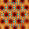
New 2D material challenges graphene
12 December 2018Graphene’s excellent electrical and thermal conductivity make it promising for electronics. The material has garnered a lot of research attention in the short time since its discovery. But the two-dimensional carbon material’s Achilles heel is the lack of a bandgap. Bandgaps, possessed by traditional semiconductor materials like silicon, are required to make the transistors that act as switching elements in logic circuits.
“Huge efforts have been devoted to open the bandgap in graphene by stretching it and/or sandwiching it with other layered materials,” says Jong-Beom Baek, a professor of energy and chemical engineering at Ulsan National Institute of Science and Technology (UNIST). But the processes are cumbersome and difficult to control, he says. So researchers are looking for new 2D materials with tunable electronic properties.
Baek and his colleagues from UNIST and Pohang University of Science and Technology have now developed a new 2D material based on graphene itself by incorporating nitrogen atoms. The new 2D crystal shares the hexagonal lattice structure of graphene, but it is riddled with uniformly distributed holes and nitrogen atoms. Nitrogen atoms replace six carbon atoms around the periphery of each hole, with a C2N stoichiometry in the basal plane. The researchers reported their findings in the journal Nature Communications.
The holey nitrogenated carbon crystal is easy to make using a simple wet chemical reaction. The researchers made a solution of hexaaminobenzene and hexaketocyclohexane, and added a few drops of sulfuric acid. This results in a dark graphite-like solid in the solution that the researchers extracted, cleaned, and freeze-dried. Scanning tunneling microscopy revealed the crystals’ structure.
The reaction of the hexa-amine and hexa-ketone monomers spontaneously generates the holey crystalline 2D network, Baek says. The new 2D crystal has a bandgap of 2.0 eV, which is larger than the 1.11 eV bandgap of silicon. “By localizing the electronic cloud around themselves and holes by creating Mott-type physical resistance, the nitrogen atoms contribute to a band-gap opening in the range of commonly used semiconductor materials,” he says.
The researchers were able to make a solution of the crystals and deposit it on rigid silica and flexible plastic substrates. The deposited films contained multiple stacked layers of the crystals. The team also demonstrated the material’s potential for electronics by using it as the semiconductor layer in a field-effect transistor. The transistors show an on/off ratio of 107, about 100 times higher than that of silicon. The on/off ratio, which correlates to the bandgap, signifies a transistor’s ability to switch current on and off.
The new work is “a major breakthrough in the design and development of 2D materials with new structures and properties,” says Liming Dai, director of the Center of Advanced Science and Engineering for Carbon at Case Western Reserve University. Producing conventional 2D materials like graphene on a large scale is challenging. But the nitrogenated crystals described here can be simply synthesized via a bottom-up wet-chemical reaction. They could be cost-effective to make on a large scale given their scalable solution synthesis method.By Prachi Patel
-
Confining LiBH4 in mesoporous silica yields solid electrolyte for Li-ion batteries
12 December 2018Lithium ion batteries surround us; they are in our phones, our laptops, and even our cars. However, these batteries are far from optimized in areas such as longer lifetimes and energy densities. One of the major challenges is the weight of the batteries. Lithium-ion batteries today are filled with liquid or gel electrolytes, a weight that can't easily be altered. In addition, the liquid is often flammable, which can be dangerous, especially during the fabrication process. A study published recently in Advanced Functional Materials shows promise for a new all-solid lithium ion battery that could potentially cut down the weight of the batteries.
"This would be a big deal for cars," says Petra E. de Jongh, a materials scientist at Utrecht University in the Netherlands and a co-author on the study. With lighter batteries in place, cars can achieve better gas mileage-a particularly important figure considering lithium ion batteries are currently used in environmentally friendly vehicles such as hybrids.
Lithium ion batteries rely on liquid or gel electrolytes for ion transport; the liquids and gels typically comprise lithium salts. Positive lithium ions shuttle between the anode and cathode of the battery upon charging and discharging, facilitating the current in the external circuit. Liquids and gels have been the go-to for battery electrolytes because ion transport is fast and reliable, says de Jongh. But beyond weight and safety issues, liquids and gels don't make for long-lived batteries. Lithium dendrites can form, stretching between electrodes resulting in short-circuits.
To create longer-lived and lighter batteries, de Jongh turned to her work with hydrogen storage materials. Replacing the liquid and gel electrolytes with a solid electrolyte would then be ideal; however, such an electrolyte would have to have high ion transport properties. For de Jongh, a metal hybrid family known as borohydrides, such as Mg(BH4)2 and LiBH4, became of interest. When used for hydrogen storage, this material had shown high efficiency in transporting ions. In collaboration with Didier Blanchard, a materials scientist at the Danish Technical University, de Jongh decided to make a leap to lithium ion transport in batteries using this material.
The researchers encased the LiBH4 in a nanoporous silica, since silica has a low ionic and electronic transport efficiency, but the shape of the pores is tunable. By creating pores of different shapes and sizes, the researchers aimed to gain a better understanding of the effects confinement had on the ion transport efficiency of LiBH4.
They created scaffolds of silica dioxide that had cylindrical pores with a volume of 0.88-0.97 cm3/g. The pores were filled with LiBH4 through melt infiltration, where the scaffold and samples of LiBH4 were autoclaved at 295°C, allowing the LiBH4 to infiltrate the scaffold. It became clear that the lithium ions were still highly mobile even at room temperature.
"[The speed] wasn't much different than what happens in a liquid," says de Jongh. The mechanism behind the fast conductance remains a bit of a mystery, she says, though it is clear that it is related to the interface between the scaffold and the LiBH4.
John B. Goodenough, a mechanical engineer at the University of Texas who also studies lithium batteries, has a theory however. He says that it's been known for some time that the introduction of oxides, such as the dioxide in the silica scaffold, allows for faster conductance of lithium ions. "The morphology of the cylindrical pores in the porous SiO2 creates connected interfacial regions for a better bulk Li+ conduction," says Goodenough, who was not affiliated with the current research.
But while the increased conductance of lithium ions in a solid electrolyte is interesting, says Goodenough, a major hurdle remains in putting it into practice. So far, all-solid batteries haven't achieved a stable interface where the solid electrolyte and the electrodes meet, he says. "This problem has so far restricted all-solid Li-ion batteries to those with thin electrodes," says Goodenough, "and, therefore, a reduced capacity of stored electrical energy."
By Prachi Patel
-
Polymer Blends with H-Bonds Increase Thermal Conductivity
12 December 2018Polymers have a number of attractive and unique qualities, such as low cost, ease of fabrication, flexibility, and lightweight. However, the low thermal conductivity of polymers limits their applications in situations where heat transfer and dissipation is crucial, such as electronics and transportation (automobiles and planes). Now, researchers at the University of Michigan (UM) have created a polymer blend with 10 times the thermal conductivity of other amorphous polymers, by engineering its thermal properties via molecular design. The researchers published their results recently in the journal Nature Materials.
"We were able to show that by engineering how polymer chains bond to each other in a blended film, we could increase the thermal conductivity by an order of magnitude," explains UM engineer Kevin Pipe, whose expertise is in microscale heat transfer. For the project, Pipe collaborated with UM materials scientist Jinsang Kim, whose work focuses on molecular design and synthesis.
In recent years, two main approaches have been taken to increase the thermal conductivities of polymers, which are normally in the range of 0.1-0.5 W m-1K -1, Pipe says. Some researchers have focused on blending polymers with fillers (metallic or ceramic particles) that have high thermal conductivity. Though this technique has resulted in thermal conductivities of 1-10 W m-1K -1, it has a few drawbacks, such as increased cost and weight of the polymer and altered electrical and optical properties.
The second method involves aligning polymer chains. But with this technique, high thermal conductivity is limited to the direction of chain orientation and the approach requires nonconventional fabrication techniques, such as electrospinning, nanoscale templating, or mechanical stretching. "Those are the main two methods," Pipe says. Until now, "not many people have looked at how to do molecular design for heat transfer in polymers."
Heat is carried through solids by vibrations. For these vibrations to carry heat efficiently through a polymer, the material's long, spaghetti-like chains need to be bonded strongly together. If they're bound loosely (which is usually the case), one polymer chain will not adequately vibrate (and propagate heat) in response to the vibration of a nearby chain. What's more, uniformly high heat conductivity in bulk polymers requires a high density of these strong bonds to be distributed homogenously throughout the material.
To achieve these features, Pipe, Kim, and their colleagues sought to find polymer blends that form hydrogen bonds, which are 10 to 100 times stronger than the van der Waals forces that normally bind polymer chains. For the H-bond-accepting polymer, they focused on polyacryloyl piperidine (PAP). And for the H-bond-donating polymer, they tested polyacrylic acid (PAA), polyvinyl alcohol (PVA), and polyvinyl phenol (PVPh).
The researchers made their blends through a standard, spin-casting fabrication method. In short, they made solutions of their two chosen polymers by dissolving them in dimethylformamide, and then mixed them together at defined molar ratios. They then spin-cast the material onto a silicon substrate, producing thin polymer-blend films.
They found that certain blends of PAP:PAA had the highest conductivity value as measured by the differential 3ω method (which measures the temperature rise across a film), containing an exceptionally homogenous, high-density distribution of strong H-bonds. "The PAP:PAA bond is strong and formed very close to the backbones of the two polymers, with no large linker groups in the way," unlike with the other polymer blends, Pipe says. Getting the correct blend ratio is key because "there is a certain mixture fraction where we maximize the number of hydrogen bonds in the system," he adds. This creates a three-dimensional network of strong bonds that facilitates heat flow in all directions. For the PAP:PAA blend, a PAP concentration of about 0.3 yielded the highest thermal conductivity of over 1.5 W m-1K-1.
Gang Chen of the Massachusetts Institute of Technology is impressed with the work. "I believe there is lots of room in engineering thermal conductivity of polymers and this is an excellent step forward," says Chen, who has previously researched improving heat conductivity in polymers by aligning molecular chains.
Baratunde Cola, a materials scientist at the Georgia Institute of Technology, says, "A method to produce bulk polymer with isotropically high thermal conductivity-achieved without a conductive filler material-has the potential to revolutionize how we dissipate heat reliably in electronic devices, and many other technological systems." Cola says that the new study is a "very important step towards realizing such breakthrough materials."
Xiaojia Wang, a materials scientist at the University of Minnesota, says that using stronger chemical linkers and a more homogenous distribution of these linkers could improve the heat conductivity of the blends, although achieving this will be challenging. "However, it opens the possibilities of synthesizing polymers that are isotropic thermal conductors and can be processed via conventional manufacturing methods," she says. "Further mass production of these kinds of polymers will have great potentials for thermal management applications."
Pipe notes that improving heat conductivity in polymers is only one possible direction for this research. "It may also be interesting to block heat transfer by reducing interchain interactions," he says. "There are applications of polymers where blocking heat transfer is important."
By Joseph Bennington-Castro