


Analog Devices Ltd
Analog Devices, Inc. operates at the centre of the modern digital economy, converting real-world phenomena into actionable insight with its comprehensive suite of analogue and mixed signal, power management, radio frequency (RF), and digital and sensor technologies. ADI serves 125,000 customers worldwide with more than 75,000 products in the industrial, communications, automotive, and consumer markets. ADI is headquartered in Wilmington, MA. Visit www.analog.com. Both Linear Technology and Maxim Integrated are now part of Analog Devices.
Analog Devices provide efficient solutions for power management and power conversion applications in the automotive, telecommunications, industrial, medical, computing, military and high-end consumer markets using high-performance analogue ICs. Our power ICs can provide unrivalled power densities and software design simulation tools to provide both fast and accurate power module and power supply designs.
Products for power management include: switching regulators, linear regulators (LDO), µModule regulators, PMIC & Multifunction, inductorless (charge pump) DC/DC converters, LED driver ICs, power control, battery management, current source, system supervisor, hot-swap controllers, monitor and control, energy harvesting, super capacitor chargers and power management evaluation kits.
-
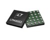
Digital Power System Manager Enables Conversion Efficiency Monitoring
17 July 2019Analog Devices announces the Power by Linear™ LTC2972, a 2-channel power system manager, featuring current, power and energy monitoring of the intermediate bus input to point-of-load (POL) converters. Monitoring circuit board power and energy use is a prerequisite for managing, optimizing and reducing their consumption in order to lower server rack and data center cooling and utility costs. The LTC2972 relieves the host of burdensome polling and computation by conveniently providing the input energy, reported in joules, and the elapsed time through a PMBus interface. When combined with its digital measurements of POL output voltages, currents, and power, the LTC2972 enables long-term monitoring of a power system’s conversion efficiency. The LTC2972 adds comprehensive software-based monitoring and control to the power systems of FPGA, ASIC, and DSP boards, accelerating time to market, enhancing system reliability, and optimizing board energy consumption.
- View the LTC2972 product page, download data sheet, order samples and evaluation boards: www.analog.com/LTC2972
Supply output voltages are trimmed, margined, and monitored using a best-in-class 16-bit analog-to-digital converter (ADC) with 0.25% total unadjusted error (TUE), improving board yields and long-term performance. Supply output currents are measured using a sense resistor, inductor DCR, or the IMON output of a power supply. Supply sequencing, supervision, and EEPROM fault-logging are built in. Faults trigger EEPROM black box recording, simplifying failure analysis while providing insight into future system improvements. Programmable power good, or general-purpose input/output (GPIO), pins are available with each channel. The LTC2972 connects with other power system managers to coordinate sequencing and fault management of more than two rails. PMBus-compatible commands are used for flexible programming and data readback of the power system. Configuration is accomplished through the LTpowerPlay® development environment, which supports all Power by Linear power system management (PSM) devices. Once programmed, no software coding is needed for autonomous operation.
Specified over the 0oC to 70oC commercial and −40oC to 105oC industrial temperature ranges, the LTC2972 is offered in a 44-pin 6mm x 7mm QFN package. Device samples and evaluation circuit boards are available online or from your local Analog Devices sales office. For more information, visit www.analog.com/LTC2972.
Summary of Features: LTC2972
- Digitally Manage Two Power Supplies
- Margin or Trim Supplies to Within 0.25% of Target Voltage
- PMBus Compliant Commands over I2C/SMBus Digital Interface
- EEPROM with ECC for Configuration & Black Box Fault Logging
- Supported by LTpowerPlay® GUI
- Supply Sequencer – Time Based, Cascade, Supports Tracking
- 16-Bit ADC with 0.25% TUE to Monitor & Obtain Telemetry on:
- Input Rail: Voltage, Current, Power & Energy
- Two Supply Outputs: Voltage, Current & Power
- Device & Two External Temperatures
- Supervise Against OV/UV Window Thresholds: Input Voltage, Two Supply Voltages,
Two External Temperatures
- Configurable Power Good Output Pins with Programmable Deglitch Delays
- Coordinate Sequencing & Fault Management across Multiple ADI PSM Devices
- Operates Autonomously without Additional Software
- Programmable Watchdog Timer
- Powered from 3.3V, or 4.5V to 15V
- –40°C to 105°C Operation
- 44-Pin 6mm × 7mm QFN Package
Pricing and Availability
Product
Production
Availability
Price Each Per 1,000
Package
Now
Start at $3.99
6mm x 7mm QFN-44
About Analog Devices
Analog Devices is the leading global high-performance analog technology company dedicated to solving the toughest engineering challenges. We enable our customers to interpret the world around us by intelligently bridging the physical and digital with unmatched technologies that sense, measure, power, connect and interpret. Visit http://www.analog.com/
-
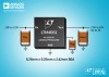
Analog Devices’ Tiny µModule Boost Regulator for Low Voltage Optical Systems
17 July 2019Analog Devices, Inc. today announced the Power by Linear™ LTM4661, a low power step-up µModule® regulator in a 6.25mm x 6.25mm x 2.42mm BGA package. Only a few capacitors and one resistor are required to complete the design, and the solution occupies less than 1cm² single-sided or 0.5cm² on double-sided PCBs. The LTM4661 incorporates a switching DC/DC controller, MOSFETs, inductors and supporting components. The LTM4661 operates from a 1.8V to 5.5V input supply, and continues to operate down to 0.7V after start-up. The output voltage can be set by a single resistor ranging from 2.5V to 15V. The combination of the small, thin package and wide input and output voltage range is ideal for a wide range of applications including optical modules, battery-powered equipment, battery-based backup systems, bias voltage for power amps or laser diodes and small DC motors.
- View the LTM4661 product page, download data sheet, order samples and evaluation boards: http://www.analog.com/LTM4661
The LTM4661 can deliver 4A continuously under 3.3VIN to 5VOUT, and 0.7A continuously under 3.3VIN to 12VOUT. The LTM4661 employs synchronous rectification, which delivers as high as 92% conversion efficiency (3.3VIN to 5VOUT). The switching frequency is 1MHz, and can also be synchronized to an external clock ranging from 500kHz to 1.5MHz. The LTM4661 1MHz switching frequency and dual phase single output architecture enable fast transient response to line and load changes and a significant reduction of output ripple voltage. The LTM4661 has three operation modes: Burst Mode® operation, forced continuous mode and external sync mode. The quiescent current in Burst Mode operation is only 25µA, which provides extended battery run time. For applications demanding the lowest possible noise operation, the forced continuous mode or external sync mode minimize possible interference of switching noise.
The LTM4661 features an output disconnect during shutdown and inrush current limit at start-up. Fault protection features include short-circuit, overvoltage and overtemperature protection.
The LTM4661 operates from –40℃ to 125℃ operating temperature. For more information, visit http://www.analog.com/LTM4661.
Summary of Features: LTM4661
- Complete Solution in <1cm² (Single-Sided PCB) or 0.5cm² (Dual-Sided PCB)
- Input Voltage Range: 1.8V to 5.5V, Down to 0.7V After Start-Up
- Output Voltage Range: 2.5V to 15V
- Up to 4A DC Output Current
- ±3% Maximum Total DC Output Voltage Regulation Over Load, Line & Temperature
- Output Disconnect in Shutdown
- Inrush Current Limit
- External Frequency Synchronization
- Selectable Burst Mode® Operation
- Output Overvoltage & Overtemperature Protection
- Ultrathin 6.25mm × 6.25mm × 2.42mm BGA package
Pricing & Availability
Product
Production
Availability
Price Each Per 1,000
Package
Now
Starts at $6.98
6.25 x 6.25 x 2.42mm BGA
About Analog Devices
Analog Devices is the leading global high-performance analog technology company dedicated to solving the toughest engineering challenges. We enable our customers to interpret the world around us by intelligently bridging the physical and digital with unmatched technologies that sense, measure, power, connect and interpret. Visit http://www.analog.com/.
Follow ADI on Twitter at http://www.twitter.com/ADI News
Subscribe to Analog Dialogue, ADI’s monthly technical journal, at:
-
Analog Devices’ Tiny µModule Boost Regulator for Low Voltage Optical Systems
17 July 2019Analog Devices, Inc. today announced the Power by Linear™ LTM4661, a low power step-up µModule® regulator in a 6.25mm x 6.25mm x 2.42mm BGA package. Only a few capacitors and one resistor are required to complete the design, and the solution occupies less than 1cm² single-sided or 0.5cm² on double-sided PCBs. The LTM4661 incorporates a switching DC/DC controller, MOSFETs, inductors and supporting components. The LTM4661 operates from a 1.8V to 5.5V input supply, and continues to operate down to 0.7V after start-up. The output voltage can be set by a single resistor ranging from 2.5V to 15V. The combination of the small, thin package and wide input and output voltage range is ideal for a wide range of applications including optical modules, battery-powered equipment, battery-based backup systems, bias voltage for power amps or laser diodes and small DC motors.
- View the LTM4661 product page, download data sheet, order samples and evaluation boards: http://www.analog.com/LTM4661
The LTM4661 can deliver 4A continuously under 3.3VIN to 5VOUT, and 0.7A continuously under 3.3VIN to 12VOUT. The LTM4661 employs synchronous rectification, which delivers as high as 92% conversion efficiency (3.3VIN to 5VOUT). The switching frequency is 1MHz, and can also be synchronized to an external clock ranging from 500kHz to 1.5MHz. The LTM4661 1MHz switching frequency and dual phase single output architecture enable fast transient response to line and load changes and a significant reduction of output ripple voltage. The LTM4661 has three operation modes: Burst Mode® operation, forced continuous mode and external sync mode. The quiescent current in Burst Mode operation is only 25µA, which provides extended battery run time. For applications demanding the lowest possible noise operation, the forced continuous mode or external sync mode minimize possible interference of switching noise.
The LTM4661 features an output disconnect during shutdown and inrush current limit at start-up. Fault protection features include short-circuit, overvoltage and overtemperature protection.
The LTM4661 operates from –40℃ to 125℃ operating temperature. For more information, visit http://www.analog.com/LTM4661.
Summary of Features: LTM4661
- Complete Solution in <1cm² (Single-Sided PCB) or 0.5cm² (Dual-Sided PCB)
- Input Voltage Range: 1.8V to 5.5V, Down to 0.7V After Start-Up
- Output Voltage Range: 2.5V to 15V
- Up to 4A DC Output Current
- ±3% Maximum Total DC Output Voltage Regulation Over Load, Line & Temperature
- Output Disconnect in Shutdown
- Inrush Current Limit
- External Frequency Synchronization
- Selectable Burst Mode® Operation
- Output Overvoltage & Overtemperature Protection
- Ultrathin 6.25mm × 6.25mm × 2.42mm BGA package
Pricing & Availability
Product
Production
Availability
Price Each Per 1,000
Package
Now
Starts at $6.98
6.25 x 6.25 x 2.42mm BGA
About Analog Devices
Analog Devices is the leading global high-performance analog technology company dedicated to solving the toughest engineering challenges. We enable our customers to interpret the world around us by intelligently bridging the physical and digital with unmatched technologies that sense, measure, power, connect and interpret. Visit http://www.analog.com/.
-
Analog Devices Announces Industrial Automation Solutions to Help Accelerate the Path to Industry 4.0
17 July 2019NORWOOD, Mass.— Analog Devices, Inc. (ADI) today announced a broad range of solutions within its advanced Industry 4.0 roadmap aimed at helping industrial equipment OEMs accelerate their path to Industry 4.0. These new solutions deliver next-generation flexibility, connectivity, and efficiency for today’s existing factory infrastructure.
“Our customers want to move fast toward Industry 4.0 but also need to ensure their investments are part of a viable, long-term plan,” said Brendan O’Dowd, general manager, Analog Devices’ Industrial Automation Business Unit. “This can be extremely difficult to navigate given the current pace of innovation. We’re focused on a set of solution areas that represent immediate opportunity for our customers to put existing brownfield infrastructure on a path to Industry 4.0. Each of the solutions we’re announcing today are critical building blocks in these strategies, which include Deterministic Ethernet, security, and condition-based monitoring.”
- Learn more about how ADI is accelerating the path to Industry 4.0: http://www.analog.com/industry4.0
Analog Devices’ New Industry 4.0 Solutions:
Device-Level Security and Time Sensitive Networking (TSN) Switching Capabilities
ADI is now providing new hardware-based identity solutions that enable security at the edge of the network within a factory control loop, and improve a field device’s security posture to meet security standards and requirements. These new capabilities are integrated with a real-time Ethernet multi-protocol switch with TSN features, including time synchronization (802.1AS) pre-emption (802.1Qbu/br), to control industrial applications via OPC-UA. By combining security capabilities with TSN features, ADI is enabling state-of-the-art field device communication solutions at the edge of industrial networks, in an easy-to-use model that accelerates customers’ time to market and adoption of Industry 4.0. To learn more on this topic, read: https://www.analog.com/en/technical-articles/tsn-in-automation-where-are-we-currently.html
ADcmXL3021 Module for Condition-based Monitoring (CbM)
The ADcmXL3021 module is a complete sensing system based on ADI’s award-winning micromechanical (MEMs) sensor technology, which increases productivity and reduces equipment repair by monitoring early indicators of machine fatigue and failure across industrial equipment and transport vehicles. This triaxial vibration sensing module combines the MEMs sensor with several signal processing functions within a compact form factor to simplify development and provide significant bill of materials savings of smart sensor nodes in CbM systems. View the product page, download data sheet, and order samples: http://www.analog.com/ADcmXL3021
High-Precision RADAR Sensors for Industrial Applications
Symeo GmbH, now part of Analog Devices, recently introduced the 60GHz Industrial RADAR Sensor Family LPR®-1DHP-200. These next-generation positioning systems feature highly precise, robust 1D distance measurements with an accuracy in the millimeter range for advanced automation, transport, and production processes. Learn more at: https://www.symeo.com/en/products/distance-measurement/new-radar-product-family-lpr-1dhp-200/index.html
Live demonstrations at Electronica 2018
ADI’s industrial automation solutions will be showcased at the ADI booth, hall C4, booth # 111 at Electronica 2018, 13-16 November in Munich, Germany.
Analog Devices have produced a dedicated event page www.analog.com/electronica that provides details of the technologies and system-level application demonstrations and solutions on view at the show.
About Analog Devices
Analog Devices is the leading global high-performance analog technology company dedicated to solving the toughest engineering challenges. We enable our customers to interpret the world around us by intelligently bridging the physical and digital with unmatched technologies that sense, measure, power, connect and interpret. Visit http://www.analog.com
All trademarks and registered trademarks are the property of their respective owners.
Follow ADI on Twitter at http://www.twitter.com/ADI_News
Subscribe to Analog Dialogue, ADI's monthly technical journal, at: http://www.analog.com/library/analogDialogue/
-
Compact 5V, 10A Synchronous Silent Switcher 2 Buck Regulator Reduces Heat, EMI & Footprint in High Power Density Applications
17 July 2019NORWOOD, MA – Analog Devices announces the Power by Linear™ LTC3310S, a 5V, 10A low EMI monolithic synchronous buck converter. The device’s fixed frequency peak current mode architecture is ideal for high step-down ratio applications that demand fast transient response. The LTC3310S uses the Silent Switcher®2 architecture with integrated hot loop bypass capacitors to deliver a highly efficient, small footprint solution at frequencies up to 5MHz with excellent EMI performance. Multiphase operation enables direct paralleling of multiple devices for higher current. The LTC3310S’ 2.25V to 5.5V input range supports a wide variety of applications, including most intermediate bus voltages. Integrated low on-resistance MOSFETs deliver continuous load currents as high as 10A with minimal thermal derating. Output voltages ranging from 0.5V to VIN are ideal for point-of-load applications such as high current/low voltage DSP/FPGA/GPU/ASIC reference designs. Other key applications include optical networking, telecom/datacom and automotive systems, distributed power architectures and general medium to high power density systems.
- View the LTC3310S product page, download the data sheet, order samples and evaluation boards: http://www.analog.com/LTC3310S
The LTC3310S’ low 35ns minimum on-time enables a high step-down ratio power supply at high frequency. 100% duty cycle operation delivers low dropout performance. The operating frequency can be synchronized to an external clock. The LTC3310S total reference voltage accuracy is ±1% over the –40°C to 125°C operating junction temperature range. Additional features include a power good signal when the output is in regulation, precision enable threshold, output overvoltage protection, thermal shutdown, die temperature monitor, clock synchronization, mode selection and output short-circuit protection. The LTC3310S is available in a thermally enhanced
18-lead 3mm × 3mm × 0.94mm LQFN package. The E- and I- grades are specified from
–40°C to 125°C operating junction temperature range. All versions are available from stock. For more information, visit http://www.analog.com/LTC3310S
Summary of Features: LTC3310S
- Silent Switcher®2 Architecture: Ultralow EMI Emissions
- High Efficiency—4.5mΩ NMOS & 16mΩ PMOS
- Wide Bandwidth, Fast Transient Response
- VIN Range: 2.25V to 5.5V
- VOUT Range: 0.5V to VIN
- VOUT Accuracy: ±1%
- Peak Current Mode Control
- 35ns Minimum On-Time
- Programmable Frequency to 5MHz
- Shutdown Current: 1µA
- Precision 400mV Enable Threshold
- Output Soft-Start with Voltage Tracking
- Power Good Output
- Die Temperature Monitor
- Configurable for Paralleling Power Stages
- Thermally Enhanced 18-Lead 3mm × 3mm LQFN Package
Pricing & Availability
Product
Production
Availability
Price Each per 1,000
Package
Now
Starts at $2.60
Thermally Enhanced
18-Lead 3mm x 3mm x 0.94mm LQFN
About Analog Devices
Analog Devices is the leading global high-performance analog technology company dedicated to solving the toughest engineering challenges. We enable our customers to interpret the world around us by intelligently bridging the physical and digital with unmatched technologies that sense, measure, power, connect and interpret. Visit http://www.analog.com.
Follow ADI on Twitter at http://www.twitter.com/ADI_News
Subscribe to Analog Dialogue, ADI’s monthly technical journal, at:
http://www.analog.com/library/analogDialogue/
All registered trademarks and trademarks are the property of their respective owners.
-
Analog Devices’ Transceivers Bring High-Def Video via Existing Vehicle Cable and Connector Infrastructure
17 July 2019NORWOOD, Mass.—Analog Devices, Inc. today announced a transceiver series that enables high-definition (HD) video over existing Unshielded Twisted Pair cables and unshielded connectors. This allows OEMs to upgrade easily from standard-definition cameras to HD cameras and provide the superior resolution and image quality required for today’s automotive camera applications. The new ADV7990 and ADV7991 transmitters and ADV7380 and ADV7381 receivers use ADI’s Car Camera Bus (C2B™) technology to enable significant savings in weight, bulk, cost, and reduce cable-routing constraints when compared to other automotive link solutions.
- View product pages, download data sheets, and order samples:
- Learn more about ADI’s C2B technology and products: http://analog.com/en/products/audio-video/car-camera-bus.html
- Connect with engineers and ADI product experts on EngineerZone®, an online technical support community: http://ez.analog.com/
The C2B transceivers are defined and designed specifically for automotive applications, which means that along with supporting excellent visual quality over the unshielded infrastructure, significant care was also taken with on-chip EMC/EMI mitigation techniques enabling full compliance to the rigorous industry mandates for EMC, EMI, and ESD robustness. The performance of the innovative cable-compensation design supports 30-meter cable runs with multiple in-line connections for resolutions up to 2 megapixels at 30 Hz or 1 megapixel at 60 Hz.
“C2B has proven to be a very cost-effective solution and provides seamless transition from mainstream low-resolution NTSC to high-definition cameras, and offers significant value to car manufacturers in reducing cable harness cost and weight,” said Motoki Kanamori, general manager, Advanced Hardware Development Dept., Cockpit Systems Business Unit, Denso Corp. “Denso is excited to work with Analog Devices and use its C2B technology to enable our scalable camera and video-connectivity solutions across vehicle lineups.”
The ADV7990/91 and ADV7380/81 transceivers feature negligible latency along with uncompressed transmission; the bidirectional control channel uses the same cable and thus incurs no additional costs. These devices support a 75-MHz pixel rate (75 MHz Y, 75 MHz C) “frozen frame” detection while the bidirectional control function supports I2C, interrupt/status and general-purpose I/O (GPIO).
Pricing and Availability
Product
Sample Availability
Production Availability
Price Each per 1,000 Units
Packaging
Technical Specifications
ADV7990
Now
January 2019
$3.60
32-LFCSP
10-bit parallel input bus
-40°C to +105°C
ADV7991
Now
November 2018
$4.00
40-LFCSP
16-bit parallel input bus
-40°C to +105°C
ADV7380
Now
January 2019
$6.00
48-LFCSP
MIPI-CSI2 transmitter
-40°C to +105°C
ADV7381
Now
November 2018
$6.00
48-LFCSP
16-bit parallel output bus
-40°C to +105°C
Live demonstration at Electronica 2018
The C2B solution will be showcased at the ADI booth, hall C4, booth # 111 at Electronica 2018, 13-16 November in Munich, Germany.
Analog Devices have produced a dedicated event page www.analog.com/electronica that provides details of the technologies and system-level application demonstrations and solutions on view at the show.
About Analog Devices
Analog Devices designs and manufactures semiconductor products and solutions. We enable our customers to interpret the world around us by intelligently bridging the physical and digital with unmatched technologies that sense, measure and connect. Visit http://www.analog.com.
C2B is a trademark of Analog Devices, Inc.
EngineerZone is a registered trademark of Analog Devices, Inc.
Subscribe to Analog Dialogue, ADI’s monthly technical journal, at: http://www.analog.com/analog-dialogue
-
Analog Devices’ Precision +/-10V and 0-20mA A/D Converters Simplify PLC Module Development
17 July 2019Analog Devices, Inc. (ADI) introduced today two multi-channel +/-10V and 0-20mA precision A/D converters that better enable implementation of programmable logic controller (PLC) and distributed control system (DCS) modules. Leveraging ADI’s iPassives® integrated precision passives technology, the AD4111 and AD4112 A/D converters integrate precision matched current sense resistors and resistor dividers. The high degree of channel-to-channel matching simplifies calibration requirements, and with support for up to eight single-ended voltage inputs and four current inputs, makes the new products ideal for use as reconfigurable platform solutions, while reducing size, complexity and cost in PLC and DCS modules.
- View the product page, download the datasheet, order samples or evaluation boards:
http://www.analog.com/AD4111 or http://www.analog.com/AD4112
- Learn more about ADI’s PLC/DCS solutions: http://www.analog.com/en/applications/markets/industrial-automation-technology-pavilion-home/plc-dcs.html
- Learn about ADI’s industry leading portfolio of precision ADCs: http://www.analog.com/en/products/analog-to-digital-converters/standard-adc/precision-adc-20msps.html
The AD4111 and the AD4112 A/D converters can accept +/-10V while meeting performance specifications and has a functional range of +/-20V, adding over-range margin to the nominal +/-10V. They can also accept currents of -0.5 to 24mA while meeting performance specifications. This allows reliable measurements close to 0mA and provides over range margin past 20mA. The devices offer an Absolute Maximum Rating of +/-50V on voltage pins and +/-50mA on current pins. The AD4111 uniquely enables open wire detection, to detect when an external sensor or signal source is disconnected from the system input, on +/-10V voltage inputs while operated from either a +5V or +3.3V single power supply.
When used in conjunction with the ADuM5411 quad-channel digital isolator, the AD4111 supports EMC/EMI standards IEC 61000-2, IEC 61000-3, IEC 61000-4, IEC 61000-5, IEC 61000-6, and CISPR 11.
AD4111 Product Highlights:
- Single 3.3V or 5V supply
- Single design supports both voltage and current inputs
- Integration of precision matched current sense resistor and resistor dividers
- +/-10V specified input voltage range and +/-20V functional input voltage range
- >1Mohm input impedance
- Enables open-wire detection
Pricing and Availability
Product
Full Production
Price Each per 1,000
Packaging
AD4111
Now
$7.25
40ld LFCSP (6x6x0.95mm)
AD4112
Now
$6.45
40ld LFCSP (6x6x0.95mm)
Now
$59.00 Each
Now
$59.00 Each
About Analog Devices
Analog Devices is the leading global high-performance analog technology company dedicated to solving the toughest engineering challenges. We enable our customers to interpret the world around us by intelligently bridging the physical and digital with unmatched technologies that sense, measure, power, connect and interpret. Visit http://www.analog.com
-
Analog Devices at European Microwave Week: Enabling the Infrastructure for 5G
17 July 2019Visitors to Analog Devices’ (ADI) stand at the forthcoming European Microwave Week 2018 (Madrid, Spain, September 25 – 29) will be able to view demonstrations and exhibits that reaffirm the company’s position as the foremost semiconductor supplier for RF, microwave and millimeter wave designs at every frequency from DC to over 100 GHz.
ADI’s stand (#135) at EuMW2018 will host the first public demonstration of several significant products released to the market in recent weeks, advancing the state-of-the-art in areas such as 5G communications, phased-array RADAR and software-configurable radio.
5G transceivers handle legacy radio standards
With its award-winning RadioVerse wideband transceivers, Analog Devices transformed the design process for the RF path in a multitude of radio products. The ADI stand at EuMW will feature the latest generation of RadioVerse chip which increases bandwidth, adds further integration and cuts power demand. The IC anticipates the upcoming need for large numbers of 5G base stations to be deployed economically; with twice the bandwidth – 200 MHz – of its predecessor and tunability over 75 MHz to 6 GHz, it will support not only 5G RF standards, but also 2G, 3G and 4G. Replacing up to 20 components and more-than-halving power demand, a demonstration of this IC will show configurable RF capability that extends beyond 5G, to a broad range of infrastructure, aerospace and defense systems.
12-bit, 10-GSPS ADCs further boost bandwidths
In analog-to-digital conversion, ADI has brought to market many successive generations of high-speed products, each time advancing performance across their specifications. To be demonstrated at EuMW, ADI’s latest 12-bit, 10.25-GSPS ADC targets next-generation communications, defense and test and measurement applications. Extended parametric performance offers greater Nyquist bandwidth supporting digitization of RF signals up to 7 GHz. The demonstration will highlight the device’s faster sampling (factor of 2.5x), improved dynamic range and superior noise performance over similar devices.
Cutting size, weight, power in phased-array RADAR
As RADAR deployments become more diverse, applications encounter limits of SWaP – size, weight and power. Phased-array RADARs are attractive for their flat-panel, no-moving-parts attributes, but demand efficient transmit/receive performance over many channels. Highlighting a newly-released device, a demonstration on the ADI stand at EuMW18 will show how integration can resolve this dilemma; analog beamforming will be shown in a system that will track visitors as they approach the exhibit. Simplifying the designers’ task, this 4-channel chip replaces multiple conventional components to build TDD RADARs operating in X and Ku bands, integrating T/R switching and providing complete support for phase-control on a per-channel basis.
High integration in a leading-edge PLL chip
The PLL (phase-locked-loop) and VCO (voltage-controlled oscillator) functions are fundamental to RF designs, more so in an increasingly digital signal-handling context. Also seen for the first time on the ADI stand at EuMW18, will be a synthesizer IC comprising a PLL with fully integrated VCO, as well as on-chip low-dropout regulators (LDOs) to provide the necessary highly stable supply rails; plus integrated tracking filter technology. The demonstration will show how the lowest levels of RMS jitter can be achieved at high output frequencies, in applications that will span aerospace and defense, test & measurement, and communications infrastructure.
Analog Devices’ applications engineers will be on hand at stand #135 to answer visitors’ questions on any aspect of RF signal chain design, building on ADI’s decades of experience at both component and system level.
Full information on European Microwave Week is available at www.eumweek.com
About Analog Devices
Analog Devices is the leading global high-performance analog technology company dedicated to solving the toughest engineering challenges. We enable our customers to interpret the world around us by intelligently bridging the physical and digital with unmatched technologies that sense, measure, power, connect and interpret. Visit http://www.analog.com
-
3.2MHz, Automotive Grade Quad 1A Step-Down Regulators + LDO Reduces Footprint & EMI
17 July 2019NORWOOD, MA – August 16, 2018 – Analog Devices announces the Power by Linear™ ADP5138, automotive qualified, high efficiency, 3.2MHz synchronous quad output buck regulators, incorporating a unique fixed frequency, peak current mode, PWM control architecture that reduces conducted and radiated emissions. The device’s high efficiency buck regulators improve thermal management, operate down to 0.8V outputs and deliver up to 1A of continuous output current from each channel. Also integrated is a 250mA low output noise (20µVRMS from 10Hz to 100kHz), high PSRR (61dB at 1kHz) low dropout linear regulator (LDO) for powering noise-sensitive devices. This high level of integration and combination of features, in addition to the compact 4mm x 4mm LFCSP package, make it ideal for automotive, industrial and instrumentation systems, as well as DC to DC point-of-load applications where space is at a premium.
- View the ADP5138 product page, download the data sheet, order samples and evaluation boards: http://www.analog.com/ADP5138
The ADP5138 runs at a fixed PWM switching frequency of 3.2MHz, or can be synchronized to the external clock from 2.8MHz to 3.5MHz, which is outside the amplitude modulation (AM) band. Furthermore, this high switching frequency reduces the size of external components, enabling a smaller solution footprint. The four buck regulators run 90° out-of-phase to each other, reducing the input ripple current and the input capacitor size and lowering the system’s electromagnetic interference (EMI). Integrated internal compensation simplifies design, and the device’s internal soft-start circuitry and power-up sequencing reduce input inrush current. The ADP5138 monitors the input voltage and provides input overvoltage lockout (OVLO), undervoltage monitor (UVM), and undervoltage lockout (UVLO) features. The device also monitors the undervoltage and overvoltage of the outputs. The power-on reset (POR) signal is asserted when the input or output voltage fault occurs. Additional protection includes overcurrent protection (OCP) and thermal shutdown (TSD).
The ADP5138 and the automotive qualified version, the ADP5138W, are offered in a low profile (0.75mm), compact 28-lead 4mm x 4mm LFCSP package with backside exposed metal pad for excellent thermal performance. The devices operate from –40°C to 125°C (junction temperature). For more information, visit http://www.analog.com/ADP5138.
Summary of Features: ADP5138
- Input Voltage: 3V to 5.5V
- Continuous Output Current
- Channel 1 to Channel 4 (Buck): 1A Each
- Channel 5 (LDO): 250mA
- 3.2MHz Fixed PWM Switching Frequency
- Synchronization Input Function
- Individual Precision Enable Input
- Power-On Reset Output
- Soft-Start & Power-Up Sequencing Reduce Inrush Current
- Active Output Discharge Function
- Input Overvoltage Lockout (OVLO), Undervoltage Monitor (UVM), & Under-voltage Lockout (UVLO)
- Thermal Shutdown (TSD)
- 28 Lead, 4mm x 4mm LFCSP Package
- Junction Temperature: –40°C to 125°C
- Qualified for Automotive Applications (ADP5138W)
Pricing & Availability
Product
Production
Availability
Price Each per 1,000
Package
Now
Starts at $2.03
4mm x 4mm LFCSP-28
Now
Starts at $2.25
4mm x 4mm LFCSP-28
-
High Precision Fixed-Gain Fully Differential Amplifiers/ADC Drivers with Low Power
17 July 2019NORWOOD, MA – August 14, 2018 – Analog Devices announces LTC6363-0.5,
LTC6363-1 and LTC6363-2 Precision, Fixed-Gain, Fully Differential Amplifiers, creating a family of ultra-precision fixed-gain variants of the successful LTC6363 amplifier. The new offerings are available in fixed gains of 0.5, 1 and 2V/V which provide flexibility when scaling inputs to the full range of ADCs.
- View the LTC6363 product page, download the data sheet, order samples and evaluation boards: http://www.analog.com/LTC6363
The precision resistors, which are integrated in LTC6363-0.5, LTC6363-1 and LTC6363-2, have been designed with overall system performance in mind, striking a balance between noise and linearity, and utilizing laser trimmed factory calibration to achieve a level of precision which is difficult and costly to achieve discretely. Initial gain accuracy is 45ppm maximum and varies by only 0.5ppm/oC maximum over temperature. Common mode rejection ratio, which is typically limited by discrete resistor matching, is an outstanding 94dB minimum, equivalent to a 0.002% resistor matching.
“One of the challenges when driving high performance SAR ADCs is finding an appropriate driver that consumes comparable power while maintaining the noise and linearity performance of the ADC. This is where the LTC6363 family excels. For example, the LTC2378-20 20-bit SAR ADC consumes 21mW at 1Msps,” says Maziar Tavakoli, Design Manager, Linear Products and Solutions. “The LTC6363 family’s noise and linearity have negligible impact on ADC performance while consuming a mere 19mW, comparable to the ADC’s power consumption. Now with the LTC6363-0.5, LTC6363-1 and LTC6363-2 you can get this same ADC driving performance plus the added precision afforded by the precision integrated resistors, all in the same compact MSOP8 package.”
The entire LTC6363 family operates with supply voltages from 2.8V (±1.4V) to 11V (±5.5V) while drawing 1.75mA typical supply current. The devices are specified for operation over a temperature range from –40°C to 125°C. The LTC6363 fixed-gain series are available in a 3mm x 5mm plastic MSOP8 package, and the LTC6363 (without resistors) is also offered in the tiny 2mm x 3mm DFN package. For more information, visit http://www.analog.com/LTC6363.
Summary of Features: LTC6363 series:
- Available with User-Settable Gain or Fixed-Gain of 0.5V/V, 1V/V, or 2V/V
- 2.9nV/√Hz Input-Referred Noise
- Drives 20-Bit SAR & Sigma-Delta ADCs
- 2mA Maximum Supply Current
- 45ppm Max Gain Error
- 0.5ppm/°C Max Gain Error Drift
- 94dB Min CMRR
- 100μV Max Offset Voltage
- 50nA Max Input Offset Current
- Fast Settling: 720ns to 18-Bit, 8VP-P Output
- 2.8V (±1.4V) to 11V (±5.5V) Supply Voltage Range
- Differential Rail-to-Rail Outputs
- Input Common Mode Range Includes Ground
- Low Distortion: 118dB SFDR at 2kHz, 18VP-P
- 500MHz Gain-Bandwidth Product
- 35MHz –3dB Bandwidth
- Low Power Shutdown: 20μA (VS = 3V)
- 8-Lead MSOP and 2mm × 3mm 8-Lead DFN Packages
Pricing & Availability
Product
Production
Availability
Price Each per 1,000
Package
Now
Starts at $2.49
8-Lead MSOP & DFN
Now
Starts at $3.92
8-Lead MSOP
Now
Starts at $3.92
8-Lead MSOP
Now
Starts at $3.92
8-Lead MSOP
-
Highly Integrated 2.5A Backup Power Manager Provides High Efficiency Charging & System Backup for up to Two Supercapacitors
17 July 2019NORWOOD, MA – August 10, 2018 – Analog Devices announces the Power by Linear™ LTC4041, a complete supercapacitor backup power management system for 2.9V to 5.5V supply rails that must be kept active during a main power failure. Supercapacitors have higher power density than batteries, making them ideal for systems requiring high peak power backup for short periods of time.
- View the LTC4041 product page, download data sheet, order samples and evaluation boards: http://www.analog.com/LTC4041
The LTC4041 uses an on-chip bidirectional synchronous converter to provide high efficiency step-down supercapacitor charging, as well as high current, high efficiency boost backup power. When external power is available, the device operates as a step-down battery charger for one or two supercapacitor cells while giving preference to the system load. When the input supply drops below the adjustable power-fail input (PFI) threshold, the LTC4041 switches to step-up regulator operation, capable of delivering up to 2.5A to the system load from the supercapacitor. During a power fail event, the device’s PowerPath™ control provides reverse blocking and a seamless switchover from input power to backup power. Typical applications for the LTC4041 include ride-through “dying gasp” supplies, high current ride-through 3V-5V uninterruptible power supplies (UPSs), power meters, industrial alarms, servers and solid-state drives.
The LTC4041 includes an optional overvoltage protection (OVP) function using an external FET which can protect the IC from input voltages greater than 60V. An internal supercapacitor balancing circuit maintains equal voltages across each supercapacitor and limits the maximum voltage of each supercapacitor to a predetermined value. Its adjustable input current limit function enables operation from a current limited source while prioritizing system load current over battery charge current. An external disconnect switch isolates the primary input supply from the system during backup. The device also includes input current monitoring, an input power fail indicator, and a system power fail indicator.
The LTC4041 is offered in a low profile (0.75mm) 24-lead 4mm x 5mm QFN package with backside metal pad for excellent thermal performance. The device operates from –40°C to 125°C, in both E and I grades. For more information, visit http://www.analog.com/LTC4041.
Summary of Features: LTC4041
- 2.5A Step-Down Supercapacitor Charger & 2.5A Step-Up Backup Supply
- 6.5A Switches for 2.5A Backup from One Supercapacitor or Two in Series
- Input Current Limit Prioritizes Load over Charge Current
- Input Ideal Diode Isolates Input During Backup
- Automatic Seamless Switchover to Backup Mode
- Internal Supercapacitor Balancer (No External Resistors)
- Programmable Charge Current & Charge Voltage
- Input Power Fail Indicator
- System Power Good Indicator
- Optional OVP Circuitry Protects Device to >60V
- Constant Frequency Operation
- Thermally Enhanced 24-Lead 4mm × 5mm QFN Package
Pricing & Availability
Product
Production
Availability
Price Each per 1,000
Package
LTC4041EUFD#PBF
Now
Starts at $2.90
24-Lead 4mm x 5mm QFN
LTC4041IUFD#PBF
Now
Starts at $3.30
24-Lead 4mm x 5mm QFN
-
High Efficiency N-Channel Switching Surge Stopper Protects Against 150V Transients
16 July 2019NORWOOD, MA – August 08, 2018 – Analog Devices announces the Power by Linear™ LTC7862, a high efficiency switching surge stopper with overvoltage and overcurrent protection for high availability systems. The LTC7862 drives an N-channel power MOSFET stage. During normal operation the LTC7862 passes the input voltage through to the output with minimal conduction loss. When an input overvoltage condition occurs, the LTC7862 starts switching as a high efficiency DC/DC regulator, protecting critical downstream components by limiting the output voltage and current.
- View the LTC7862 product page, download data sheet, order samples and evaluation boards: http://www.analog.com/LTC7862
The LTC7862 builds on popular linear surge stoppers such as the LTC4363 by offering high efficiency switching protection to extend output current capability and reduce power loss during transients and faults. Supply voltages surge when the load current changes abruptly in long inductive power busses. The situation is aggravated in automotive applications by the energy stored in the alternator’s inductance, causing an elevated and extended voltage surge during a load dump. The power handling capability of a surge stopper is limited by the power lost in the protection circuit. In a linear surge stopper, the power capability is determined by the size of the pass MOSFET, while in a switching surge stopper the power capability is determined by conversion efficiency. Due to its lower power loss, a switching surge stopper can operate through longer input voltage surges at higher output current than a linear solution.
The LTC7862 has an input voltage operating range of 4V to 140V, 150V abs max. An external fault timer capacitor configures the limited time spent in overvoltage mode and keeps the switching surge stopper below a safe peak operating temperature when power loss is at its highest levels. The fault timer saves system cost and size by allowing component selection to be optimized for normal mode rather than overvoltage transient and fault conditions.
In MIL-STD-1275 applications the LTC7862 protects devices operating from a 28V vehicle power bus, where this bus voltage can reach as high as 100V and last up to 500ms. The LTC7862 also fits into industrial, avionics, and automotive power, including ISO 7637.
The LTC7862 is available in 20-Lead 4mm × 5mm QFN and TSSOP packages. Three temperature grades are available, with operation from –40 to 125°C for the extended and industrial grades and a high temp automotive grade of –40°C to 150°C. For more information, visit www.analog.com/LTC7862.
Summary of Features: LTC7862
- VOUT Clamp Stops High Voltage Input Surges
- 100% Duty Cycle Pass-Through Mode During Normal Operation
- Switches During Overvoltage or Overcurrent Transients, Faults & During Start-Up
- High Efficiency Switching Enables Long Duration Surge Protection
- Wide VIN Range: 4V to 140V (150V Abs Max)
- Adjustable Output Voltage Clamp Up to 60V
- Adjustable Output Overcurrent Protection
- RSENSE or Inductor DCR Current Sensing
- Power Inductor Reduces Input EMI in Normal Mode
- Adjustable Soft-Start for Inrush Current Limiting
- MIL-STD-1275 & ISO 7637 Compatible
Pricing & Availability
Product
Production
Availability
Price Each Per 1,000
Packages
Now
Starts at $3.40
20-Lead 4mm × 5mm QFN & TSSOP
-
Highly Programmable Super Sequencer Simplifies Multi-Rail Power System Management
16 July 2019NORWOOD, MA – August 06, 2018 – Analog Devices announces the Power by Linear™ ADM1266 Super Sequencer®, a highly programmable device for monitoring, sequencing, and margining up to 17 power supplies. For larger rail counts, a proprietary 2-wire interdevice bus synchronizes the operation of 16 ADM1266s. A built-in sequencing engine monitors each supply fault detector, general purpose inputs/outputs, and timers to turn the supplies on and off in a user-determined sequence. All configuration is performed through the intuitive ADI Power Studio GUI, reducing design time. The ADM1266 provides a highly flexible yet simple solution to manage complex power systems on FPGA, ASIC, and processor boards in network routers and switches, servers and data storage systems.
- View the ADM1266 product page, download data sheet, order samples and evaluation boards: http://www.analog.com/ADM1266
The ADM1266 integrates an analog-to-digital converter (ADC) and nine voltage output digital-to-analog converters (DACs) that adjust the feedback node or reference of a DC-to-DC converter to implement a closed-loop, autonomous margining system. A nonvolatile EEPROM records voltage, time, and fault information when instructed by the sequencing engine configuration, speeding fault debug.
The ADM1266, along with the ADI Power Studio software, offers a feature-rich configurable state machine to meet complex sequencing requirements. Built-in debugging features like breakpoints and black box, along with the software setup wizards, reduce development and debug time from days to a matter of hours. The interdevice bus between multiple ADM1266s ensures they perform like a single device, providing for an intuitive design process. By handling all complexity, the software fashions a seamless design experience from 17 rails to 257 rails.
Specified over the −40oC to 85oC temperature range, the ADM1266 is offered in a 64-pin 9mm x 9mm LFCSP package. Device samples and evaluation circuit boards are available online or from your local Analog Devices sales office. For more information, visit www.analog.com/ADM1266.
Summary of Features: ADM1266
- Margins, Trims, Sequences, Supervises & Monitors Supplies
- Supervises, Sequences & Monitors 17 Supplies
- 257 Supplies with Cascaded ADM1266
- 2-Wire Interdevice Bus for Cascading
- Fully Programmable Sequencing Engine
- Industry Standard PMBus Interface
- EEPROM for Nonvolatile Configuration & Black Box Fault Recording
- Main & Backup Memory
- Supported by ADI Power Studio
- 12-Bit ADC for Readback of Supply Output Voltages
- 9 Voltage Output 8-Bit DACs for Supply Voltage Margining
- Powered from Highest of Two 3V–15V Inputs
- 16 PDIOs & 9 GPIOs
Pricing & Availability
Product
Production
Availability
Price Each per 1,000
Package
Now
$11.99
9mm x 9mm LFCSP-64
-
60V Low IQ Buck Controller Plus 4-Channel 8A Configurable Buck DC/DCs
16 July 2019NORWOOD, MA – August 02, 2018 – Analog Devices, Inc. announced today the Power by Linear™ LTC3372, a highly integrated power management solution for systems that require multiple low voltage outputs generated from an input voltage as high as 60V. The LTC3372 features a 60V synchronous buck switching regulator controller followed by four configurable synchronous monolithic buck regulators. This combination provides up to five high efficiency low quiescent current outputs in a single IC, ideal for automotive, industrial and medical applications.
- View the LTC3372 product page, download data sheet, order samples and evaluation boards: http://www.analog.com/LTC3372
The LTC3372’s buck controller operates over a 4.5V to 60V input voltage range and drives an all N-channel MOSFET power stage. Its output can be programmed to either 3.3V or 5V and can generate an output current up to 20A. The controller output is typically used to feed the four monolithic buck regulators. Each monolithic buck channel can be programmed to regulate an output voltage as low as 0.8V with a configurable output current up to 4A. Eight 1A integrated power stages are programmed by the C1-C3 pins into one of eight unique configurations, from a quad 2A buck to a dual 4A buck. This allows only one inductor per channel.
The LTC3372 offers a low IQ solution ideal for battery-powered or automotive applications in which one or more power supply rails are always on. With just the high voltage controller enabled, the device draws 15µA from a 12V input supply while regulating the output to 5V at no load. Each monolithic buck regulator adds only 8µA of additional IQ per channel enabled. The LTC3372’s monolithic buck switching frequency can be programmed from 1MHz to 3MHz and can be synchronized to an external clock while the buck controller switches at 1/6 of this frequency. Additional features include foldback current limiting, soft-start, short-circuit protection and output overvoltage protection.
The LTC3372 is available from stock in a thermally enhanced 48-pin 7mm x 7mm QFN package. E and I grades are specified over an operating junction temperature range of –40°C to 125°C, and the H grade features operation from –40°C to 150°C. For more information, visit www.analog.com/LTC3372.
Summary of Features: LTC3372
- High Voltage Buck Controller: VIN = 4.5V to 60V, VOUT = 5V/3.3V
- Low Voltage Buck Regulators: VINA-H = 2.25V to 5.5V, VOUT1-4 ≥ 0.8V
- 8×1A LV Buck Integrated Power Stages, Configurable as 2, 3 or 4 Output
- 8 Unique Output Configurations (1A to 4A per Channel)
- Low Total No-Load Input Supply Current (IQ)
- 15μA HV Controller Only (5VOUT)
- 23μA HV Controller Only (3.3VOUT)
- 9μA Per Additional LV Regulator Channel
- 1MHz to 3MHz Operation (HV Controller Runs at 1/6 Frequency)
- Programmable Frequency or Synchronizable to External Clock
- Programmable Watchdog & Power-On Reset Delay
- IC Die Temperature Monitor Output
- Thermally Enhanced 48-Pin 7mm x 7mm QFN Package
Pricing & Availability
Product
Production
Availability
Price Each per 1,000
Package
Now
Starts at $5.75
Thermally Enhanced 7mm x 7mm
48-Lead QFN
-
Analog Devices and B-Secur Collaborate on Biometric Authentication Technologies for the Automotive Industry
16 July 2019NORWOOD, Mass.-- Analog Devices, Inc. (ADI) announced today a collaboration with B-Secur LTD to develop a complete biometric authentication solution for use in automotive vehicles. The combination of ADI’s leading signal conditioning technology with B-Secur’s electrocardiogram (ECG) biometric algorithms software will enable automobiles to uniquely authenticate and identify drivers and passengers. The technology is designed to detect driver readiness and wellness by monitoring the driver’s vital signs for any irregularities. In addition, the ECG identification capability can be used to access features such as vehicle entry, immobilizer deactivation, infotainment personalization and online payments for ridesharing usage, personalized insurance payments and more.
- Learn more details about the ADI/B-Secur collaboration: https://www.b-secur.com/b-secur-at-car-hmi/
- Learn more about ADI’s offerings for the automotive market:
http://www.analog.com/en/applications/markets/automotive-pavilion-home.html
“B-Secur’s ECG biometric technology can not only quickly and securely verify identity, but also turn the data into meaningful insights on driver/passenger wellness, including stress and drowsiness,” said Ben Carter, chief commercial officer, B-Secur. “We are delighted to collaborate with Analog Devices to help make the world a safer place with ECG biometrics, securing human and technology interaction at its heart.”
-
Sigma-Delta A/D Converter Provides Single Configurable & Reusable Data Acquisition Footprint for AC & DC Performance
16 July 2019NORWOOD, MA – July 30, 2018 – Analog Devices, Inc. today introduced the AD7768-1, a low power, high-performance, 24-bit single channel sigma-delta (ƩΔ) A/D for precision conversion of both AC and DC signals. AD7768-1 enables power efficient instrumentation solutions for condition monitoring in predictive maintenance (vibration and power quality), audio test, acoustic, structural health and modular automated electrical test equipment. Healthcare applications such as clinical EEG/EMG/ECG are also enabled.
The AD7768-1 provides a single configurable and reusable data acquisition footprint, establishing a new industry standard in combined AC and DC performance. This enables instrumentation and industrial system designers in reuse of core acquisition chain which can service multiple measurement variants, both in channel to channel isolated and non-isolated applications. A single converter serving the various equipment platforms, performance points and measurement ranges reduces the number of reference designs, reducing costs and time to market.
The AD7768-1 includes a power scalable ƩΔ modulator and digital filter to enable synchronized, high-fidelity measurement of AC and DC signals in instrumentation. The high throughput and 110.8kHz input bandwidth of the AD7768-1 deliver test cost and time reduction, improving the quality and integrity of test measurements.
The AD7768-1 offers extensive digital filtering capabilities, which can be selected to meet a wide range of system requirements catering to high accuracy frequency domain measurements and low latency DC input measurement. The ADC also provides an integrated pre-charge buffer on each analog input, greatly simplifying the design of external driver circuitry. A full buffer input on the reference delivers a high impedance input for any external reference.
- View product page, download data sheet, order samples and evaluation boards: http://www.analog.com/AD7768-1BCPZ
- Connect with engineers and experts on EngineerZone®, an online technical support community: https://ez.analog.com/community/data_converters
The 24-bit AD7768-1 delivers the industry’s best integral nonlinearity (INL) and lowest distortion performance across the widest available bandwidth. It also achieves 20 times better offset drift, 40 times reduction in gain error, and a 3-time improvement in gain drift over alternative products. Choosing the correct ADC driver is important in obtaining the maximum performance from the AD7768-1. Find appropriate ADC driver here: http://www.analog.com/en/products/amplifiers/adc-drivers.html
Pricing & Availability
Product
Output Data Rate
Resolution
Availability
Price Each per 1,000
Packaging
256kSPS
24-Bit
Now
$5.95
28-Lead LFCSP
-
3.2A, 35VIN/35VOUT Synchronous Monolithic Multi-Chemistry PowerPath Manager/Charger Features Digital I2C Telemetry & MPPT Operation
16 July 2019NORWOOD, MA – July 27, 2018 – Analog Devices announces the Power by Linear™ LTC4162, a highly integrated, high voltage multi-chemistry synchronous monolithic step-down battery charger and PowerPath™ manager with onboard telemetry functions and optional maximum power point tracking (MPPT). The LTC4162 efficiently transfers power from a variety of input sources, such as wall adapters, backplanes and solar panels, to charge a Li-Ion/Polymer, LiFePO4 or lead-acid battery stack and provide power to a system load up to 35V. The device provides advanced system monitoring and PowerPath management, plus battery health monitoring. While a host microcontroller is required to access the most advanced features of the LTC4162, the use of the I2C port is optional. The main charging features of the product can be adjusted using pin-strap configurations and programming resistors. The device offers precision ±5% charge current regulation up to 3.2A, ±0.75% charge voltage regulation and operates over a 4.5V to 35V input voltage range. Applications include portable medical instruments, USB power delivery profile 1-5 devices, military equipment, industrial handhelds and ruggedized notebook/tablet computers.
- View the LTC4162 product page, download data sheets, order samples and evaluation boards: www.analog.com/LTC4162
The LTC4162 contains an accurate 16-bit analog-to-digital converter (ADC) that continuously monitors numerous system parameters on command, including input voltage, input current, battery voltage, battery current, output voltage, battery temperature, die temperature and battery series resistance (BSR). All system parameters can be monitored via a 2-wire I2C interface, while programmable and maskable alerts ensure that only the information of interest causes an interrupt. The device’s active maximum power point tracking algorithm globally sweeps an input undervoltage control loop and selects an operating point to maximize power extraction from solar panels and other resistive sources. Further, the LTC4162’s PowerPath topology decouples the output voltage from the battery, thereby allowing a portable product to start-up instantly when a charging source is applied under very low battery voltage conditions.
The LTC4162’s onboard charging profiles are optimized for each of a variety of battery chemistries, including Li-Ion/Polymer, LiFePO4 and lead acid. Both charge voltage and charge current can be automatically adjusted based on battery temperature to comply with JEITA guidelines, or custom settings.
The LTC4162 is housed in a 28-lead, 4mm x 5mm QFN package with an exposed metal pad for excellent thermal performance. E- and I-grade devices are guaranteed for operation from –40°C to 125°C. All devices are available from stock. For more information, visit http://www.analog.com/LTC4162.
Summary of Features: LTC4162
- Multi-Chemistry Battery Charger with Termination (Li-Ion/Polymer, LiFePO4 &
Lead Acid)
- Wide Charging Input Voltage Range: 4.5V to 35V
- High Efficiency Synchronous Operation
- 16-Bit Digital Telemetry System Monitors VBAT, IBAT, RBAT, TBAT, TDIE, VIN, IIN, VOUT
- Input Undervoltage Charge Current Limit Loop
- Maximum Power Point Tracking (MPPT) for Solar Panel Inputs
- Input Current Limit Prioritizes System Load Output
- Low Loss PowerPath™ Manager
- Instant-On Operation with Discharged or Missing Battery
- JEITA & Lead-Acid Continuous Temperature Controlled Charging
- Thermally Enhanced 28-Pin 4mm x 5mm QFN Package
Pricing & Availability
Product
Production
Availability
Price Each per 1,000
Package
Now
Starts at $2.95
28-Pin 4mm x 5mm x 0.75mm QFN
-
50A µModule Regulator Scalable to 250A Runs Cool with Inductors Exposed as Heatsinks
16 July 2019NORWOOD, MA – July 26, 2018 – Analog Devices announces the Power by Linear™ LTM4678 dual 25A or single 50A step-down µModule® regulator with PMBus digital interface. By stacking and exposing its two inductors on top of BGA package, the LTM4678 uses the inductors as heat sinks to transfer heat from inside, keeping the device cool. Onboard EEPROM and PMBus I2C enables a user to measure, alter and record key power parameters such as voltage, load current, temperature and sequencing. Five LTM4678s can current share at 50A each to deliver up to 250A to loads such as processors, FPGAs and ASICSs. Applications include PCIe boards, communication infrastructure, cloud computing, optical as well as medical, industrial and test and measurement devices.
- View the LTM4678 product page, download data sheet, order samples and evaluation boards: http://www.analog.com/LTM4678
The LTM4678 integrates a DC/DC controller, EEPROM, power FETs, inductors and supporting components in a 16mm x 16mm x 5.86mm BGA package. Output voltage accuracy of ±0.5% is guaranteed over line, load and temperature
(–40°C to 125°C).
The LTM4678 operates from 4.5V to 16V input range, and the two output voltages are digitally controlled from 0.5V to 3.3V. The LTM4678 achieves 90% peak efficiency from 12VIN and 0.9VOUT at 50A. It delivers 40A at 12VIN to 0.9VOUT at 70°C ambient with 200LFM air flow. The switching frequency is 350kHz to 1MHz and can be synchronized to an external clock from 350kHz to 1MHz for noise sensitive applications.
The LTM4678’s high power density and scalability make it ideal for the PCB area constraints of densely populated system boards to power the low-voltage & high-current advanced digital devices. For more information, visit www.analog.com/LTM4678.
Summary of Features: LTM4678
- PMBus Digital Interface for Control, Telemetry & Monitoring of Operating Parameters
- Dual 25A or Single 50A Output Current with Current Sharing & Scalable up to 250A
- Wide Input Voltage Range: 4.5V to 16V
- Output Voltage Range: 0.5V to 3.3V
- ±0.5% Voltage Set Point Accuracy & ±5% Current Readback Accuracy
- Onboard EEPROM
- Thermally Enhanced 16mm x 16mm x 5.86mm BGA Package
Pricing & Availability
Product
Production
Availability
Price Each per 1,000
Package
Now
Starts at $47.48
Thermally Enhanced 16mm x 16mm x 5.86mm BGA
-
150V Step-Down DC/DC Controller Draws Only 9µA in Battery-Powered Systems
16 July 2019NORWOOD, MA – July 24, 2018 – Analog Devices announces the Power by Linear™ LTC3894, a high voltage step-down DC/DC controller that draws only 9µA quiescent current with the output enabled in Burst Mode® operation. Its wide 4.5V to 150V input voltage range can effectively eliminate the need for external surge suppression devices. The LTC3894’s 100% duty cycle capability and externally adjustable power good window are ideal for use in battery powered systems that operate continuously in dropout. The LTC3894 is well suited for transportation systems, always-on power, industrial control, robotic and datacom applications.
- View the LTC3894 product page, download data sheet, order samples and evaluation boards: http://www.analog.com/LTC3894
The LTC3894 drives a P-channel MOSFET power stage and can produce an output voltage from 0.8V to 60V at output currents up to 3 amps with efficiencies as high as 92%. The LTC3894 includes the option for an external N-channel pass FET to supply the PMOS gate driver current in sustained high voltage high power applications.
The LTC3894 operates with a selectable fixed frequency between 50kHz and 850kHz and is synchronizable to an external clock from 75kHz to 800kHz. The user can select between pulse-skipping or Burst Mode operation during light loads. Its current mode architecture provides easy loop compensation, fast transient response and excellent line regulation. Current sensing is accomplished by measuring the voltage drop across the output inductor (DCR) for highest efficiency or by using an optional sense resistor. A low 100ns minimum on-time allows for high step-down ratios at high switching frequency. Current foldback limits MOSFET heat dissipation during overload conditions. Additional protection features include, a power good output signal, adjustable input overvoltage lockout and soft-start.
The LTC3894 is available in a 16-pin thermally enhanced TSSOP with high
voltage pin spacing. Extended and industrial versions are available from –40°C to 125°C. For more information, visit www.analog.com/LTC3894.
Summary of Features: LTC3894
- Wide Input Voltage Range: 4.5V to 150V
- Wide VOUT Range: 0.8V to 60V
- Low 9µA Burst Mode® VIN Quiescent Current, when Regulating from 48V to 3.3V
- RSENSE or Inductor DCR Current Sensing
- Programmable Power Good Undervoltage Monitor
- Internal Fixed Soft-Start or Externally Programmable Soft-Start or Voltage Tracking
- Selectable Fixed Operating Frequency from 50kHz to 850kHz
- PLL Synchronizable Operating Frequency from 75kHz to 800kHz
- Current Mode Control for Fast Transient Response & Easy Loop Compensation
- Adjustable Soft-Start or Tracking
- Output Overvoltage & Overcurrent Protection
- Power Good Output Signal
- Optional External NMOS for Gate Driver Bias Current
Pricing & Availability
Product
Production
Availability
Price Each Per 1,000
Package
Now
Starts at $2.55
16-Pin Thermally Enhanced TSSOP
-
50A or Dual 25A µModule Regulator
10 July 2019MILPITAS, CA – February 29, 2016 – Linear Technology Corporation introduces the LTM4650, a dual 25A or single 50A output step-down µModule® regulator with onboard shielded inductors, MOSFETs and a dual DC/DC regulator IC housed in a small thermally enhanced plastic package. The device is offered in a 16mm x 16mm x 5.01mm BGA with a patented built-in heat sink. The heat sink, attached to the MOSFETs and inductors, rapidly moves heat from the interior of the package to the top, where the surface of the heat sink is exposed to air. Thermal dissipation is further improved with airflow, or a combination of airflow and attachment to an external heat sink. With no external heat sink, the LTM4650 delivers 50A from 12VIN to 0.9VOUT at up to 71°C ambient temperature with 200LFM airflow or up to 77°C with 400LFM.
The LTM4650’s precision current-mode architecture allows four devices to multiphase current share, delivering up to 200A to loads such as ASICs, FPGAs and microcontrollers. DC/DC conversion efficiency is improved by using Linear Technology’s DC/DC regulator IC with strong gate drivers and low loss MOSFETs. Delivering 50A, 92% efficiency is recorded at 5VIN, 1.8VOUT and 86% at 12VIN, 1.0VOUT.
With a differential remote sense amplifier to compensate for voltage drop due to circuit board trace impedance, the LTM4650 guarantees ±1.5% maximum total DC output voltage accuracy over line, load and temperature.
The LTM4650 is rated for operation from –40ºC to 125ºC. The 1,000-piece price starts at $46.75 each. For more information, visit www.linear.com/product/LTM4650.
-
Isolated 4-Port Power over Ethernet PSE Controller Passes IEEE 802.3bt Conformance Tests
10 July 2019NORWOOD, MA – July 23, 2018 – Analog Devices announces the Power by Linear™ LTC4291/92 isolated 4-port power source equipment (PSE) controller chipset, the first of its kind to pass a series of IEEE 802.3bt (PoE++) Power over Ethernet (PoE) conformance tests administered by Sifos Technologies. PoE naturally presents system and network engineers with PSE evaluation challenges. PSEs are multichannel, intelligent DC power sources that are activated and deactivated through standardized processes without disrupting traditional Ethernet data transmission. At the same time, compliance testing is complicated by requirements to operate over several delivery and polarity configurations.
- View the LTC4291/92 product page, download data sheet, order samples and evaluation boards: http://www.analog.com/LTC4291
The Sifos 24-port PSA-3000 PowerSync analyzer equipped with multiple 2-port PSA-3202 test blades provides complete automated testing and analysis of LTC4291/92-based PSEs. Rigorous compliance test suites augmented by specialized analysis features validated the LTC4291/92 to the IEEE 802.3at (PoE+) standard, the upcoming 802.3bt standard, and other proprietary specifications. These scalable design and test solutions build in extensive PoE knowledge and years of experience, reducing time-to-market and enabling deployment of IEEE 802.3bt PoE networks as the standard approaches ratification in 2018.
In testing performed by Analog Devices, the LTC4291/92 PSE chipset passed a wide variety of tests as the PSA-3000/3202 solution emulated a variety of IEEE 802.3bt PDs (powered devices). Continuous 90W 4-pair PSE loading capability ensured that the PSE could handle 802.3bt’s 71.3W maximum PD power level in either single- signature or dual-signature PD configurations. The LTC4291/92 correctly identified all physical layer classes (up to 5 events) as required by the new Type 3 and Type 4 PDs, as well as the backward compatible Type 1 and Type 2 PDs. For PSEs that use the link layer discovery protocol (LLDP), the PSA-3000/3202 can also emulate and analyze this type of power negotiation.
Customers configure and interact with the devices using provided GUIs and scripting environments. The LTC4291/92 is supported with lab-tested schematics, complete reference designs, the QuikEval™ GUI and example code, while the
PSA-3000/3202 is extended with the PSA Interactive GUI and PowerShell PSA scripting environment.
The LTC4291/92 chipset is offered in commercial and industrial temperature ranges. The LTC4291 digital controller is offered in a RoHS-compliant 24-pin 4mm x 4mm QFN package, while the LTC4292 analog controller is in a 40-pin 6mm x 6mm QFN package. The LTC4291/92 is Analog Devices’ first 802.3bt PSE controller and provides an upgrade path for the popular LTC4266 4-port 802.3at PSE controller. Please visit http://www.analog.com/PoE for more product information.
Pricing & Availability
Product
Production
Availability
Price Each per 1,000
Package
LTC4291 Now Starts at $2.00 24-Pin 4mm x 4mm QFN
LTC4292 Now Starts at $6.00 40-Pin 6mm x 6mm QFN
About Analog Devices
Analog Devices is the leading global high-performance analog technology company dedicated to solving the toughest engineering challenges. We enable our customers to interpret the world around us by intelligently bridging the physical and digital with unmatched technologies that sense, measure, power, connect and interpret. Visit http://www.analog.com.
-
Analog Devices’ DSP Creates Internal and External Engine Sound for Electric and Hybrid Electric Vehicles
10 July 2019NORWOOD, Mass. -- Analog Devices, Inc. (ADI) today introduced an embedded system for generating engine sound for electric (EV) and hybrid electric vehicles (HEV). The ADSP-BF706 digital signal processor and Electric Vehicle Warning Sound System (EVWSS) firmware enables automobile manufacturers in North America and other global regions to comply with future safety regulations mandating external engine sound for EVs and HEVs travelling at low speeds.
- View the EVWSS product page: http://www.analog.com/evwss
- Download EVWSS firmware by submitting a request to http://www.analog.com/srf. Please specify EVWSS.2.0.0 in the additional comments field in the software request form.
The ADI solution includes a complete hardware and firmware reference design. It can be scaled for high performance with the ADSP-BF706 or entry level applications with the ADAU1450 Digital Audio Processor. The ADSP-BF706 can also be used to create in-cabin engine sound to contribute to an improved driving experience for vehicle owners. The ADSP-BF706 uses memory mapped quad SPI memory providing faster and simpler access to the stored audio files used to create the engine sound. It can access up to 24 WAV files simultaneously, compared to conventional products that can typically access only five.
ADI’s Sigma Studio Integrated Development Environment (IDE) enables OEMs to graphically tune the audio sound when using the ADAU1450. This allows sound engineers with minimal programming experience to optimize audio performance while reducing development time. A new release of Sigma Studio supporting the ADSP-BF706 is due later this year. In addition, a low-cost CAN software stack runs on the ADSP-BF706 to help customers quickly build automotive-grade prototypes.
ADSP-BF706 Product Highlights
- Blackfin+ core with up to 400-MHz performance
- Dual 16-bit or single 32-bit MAC support per cycle
- 16-bit complex MAC and many other instruction set enhancements
- Instruction set compatible with previous Blackfin products - On-Chip Memory
- 136KB L1 SRAM with multi-parity-bit protection (64KB instruction, 64KB data, 8KB scratchpad)
- 1MByte on-chip L2 SRAM with ECC protection
- 512KByte On-chip L2 ROM - Key Peripherals include
- USB2.0 HS OTG
- 2x CAN2.0B
- ePPI Video I/O
- 2x SPORTs (w/I2S)
- 2xQuad-SPI / 1xDual-SPI (w/ Host mode)
- 12C
- 2xUART- SD/SDIO/MMC (4-bit)
Pricing and Availability
Product
Full Production
Price Each Per 1,000
Packaging
ADSPP-BF706
Now
$8.38
88-Lead LFCSP
ADAU1450
Now
$4.22
72-Lead LFCSP
About Analog Devices
Analog Devices is the leading global high-performance analog technology company dedicated to solving the toughest engineering challenges. We enable our customers to interpret the world around us by intelligently bridging the physical and digital with unmatched technologies that sense, measure, power, connect and interpret. Visit http://www.analog.com.
-
Wideband Microwave Synthesizer Delivers Industry Leading Phase Noise, Output Power and Spur Performance with Operation from 55 MHz to 15 GHz
10 July 2019NORWOOD, Mass.--Analog Devices, Inc. (ADI) announced today a wideband synthesizer with an integrated voltage-controlled oscillator (VCO) that delivers breakthrough performance and flexibility and is ideal for diverse market applications such as aerospace and defense, wireless infrastructure, microwave point-to-point links, electronic test and measurement, and satellite terminals. ADI’s new ADF5610 wideband fractional-N synthesizer generates RF outputs from 55 MHz to 15 GHz and provides the industry’s lowest phase noise performance on a single chip. When compared to alternative solutions that require multiple narrowband GaAs voltage controlled oscillators and phase-locked loops (PLLs), the ADF5610 offers 50% less power dissipation, smaller footprint and simpler architecture which translates into bill of materials cost savings and reduced time to market.
- View the ADF5610 product page, download data sheet, order samples and evaluation boards: http://www.analog.com/adf5610
Developed on ADI's proprietary advanced SiGe BiCMOS process, the ADF5610 enables high modulation bandwidths and low BIT error rates. It features industry leading VCO phase noise (-114 dBc/Hz @ 100 kHz offset and -165 dBc/Hz @ 100 MHz offset both at 10GHz) and low normalized phase noise floor (FOM) of -229 dBc/Hz. The integrated PLL function provides fast frequency hopping and lock times (<50 μs with appropriate loop filter). The phase detector spurious levels are below -45 dBc typical, and the RF output power level is 6 dBm.
The ADF5610 wideband fractional-N synthesizer is easy to design-in, and fully supported by the ADIsimPLL™, Analog Devices' comprehensive and easy-to-use PLL synthesizer design and simulation tool for assessing phase noise, lock time, jitter and other design considerations. The device is also customer programmable through the use of integrated SPI interface and control software.
The ADF5610 is specified over the -40°C to +85°C range. It operates from nominal 3.3-V analog and digital power supplies as well as 5-V charge-pump and VCO supplies, and feature 1.8-V logic-level compatibility. The synthesizer also contains hardware and software power down modes.
-
38VIN, 10A Boost µModule Regulator Ideal for Driving LEDs
10 July 2019NORWOOD, MA – July 13, 2018 – Analog Devices announces the Power by Linear™ LTM8005 boost DC/DC µModule® (power module) regulator designed for driving LEDs. The LTM8005 includes a DC/DC controller, power switch, Schottky diode and current sense resistor in a 9mm x 11.25mm x 2.22mm BGA package. The LTM8005 operates from a 5V to 38V input voltage range and can deliver up to 1.6A of regulated current at an output voltage of up to 38V. An Inductor is external, enabling the LTM8005 to easily configure in different operation modes including boost, buck-boost, buck and SEPIC topologies with a coupled inductor.
- View the LTM8005 product page, download data sheet, order samples and evaluation boards: www.analog.com/LTM8005
The high reliability H-grade version guarantees operation from –40°C to 150°C. The wide input voltage range and 150°C operation make this µModule LED driver ideal for automotive and industrial lighting applications.
The operating frequency is adjustable from 100kHz to 1MHz, and built-in spread spectrum frequency modulation improves electromagnetic compatibility performance. Brightness of the LEDs can be controlled by the analog CTRL pin and by PWM dimming with a range up to 3,000:1. The LTM8005 provides safety features such as output disconnect short-circuit protection, open LED protection, programmable input current limit, as well as, input and output current reporting.
The E and I grades of the LTM8005 operate from –40°C to 125°C, and up to 150°C for the H grade. For more information, visit www.analog.com/LTM8005.
Summary of Features: LTM8005
- Wide Input Voltage Range: 5V to 38V
- 40V, 10A Internal Power Switch
- 3,000:1 True Color PWM™ Dimming
- Internal 40V Switch for PWM & Output Disconnect
- Internal Spread Spectrum Frequency Modulation
- Open LED Protection with OPENLED Flag
- Short-Circuit Protection with SHORTLED Flag
- Input & Output Current Reporting
- 9mm x 11.25mm x 2.22mm BGA Package
-
Triple Output, Buck/Buck/Boost Synchronous DC/DC Controller Operates up to 2.25MHz in Automotive Start/Stop Systems with 28μA IQ
10 July 2019NORWOOD, MA – January 29, 2018 – Analog Devices announces the Power by Linear™ LTC7815, a high frequency (up to 2.25MHz) triple output (buck, buck, boost), synchronous DC/DC controller that maintains all output voltages in regulation during automotive cold crank conditions. A 12V automotive battery can droop to less than 4 volts during engine restart or cold crank, causing reset of infotainment systems and other electronics that operate from 5 volts and higher. The high efficiency synchronous boost converter feeds the two step-down converters, avoiding output voltage dropout when the car battery voltage droops, a useful feature in automotive start/stop systems that shut off the engine at idle to save fuel. Alternatively, the buck controllers can be powered from the input for a general-purpose triple output controller.
- View the LTC7815 product page, download data sheet, order samples and evaluation boards: www.linear.com/product/LTC7815
The LTC7815 operates from an input voltage of 4.5V to 38V during start-up and maintains operation down to 2.5V after start-up. The synchronous boost converter can produce output voltages up to 60V and can run with the synchronous switch fully ON at 100% duty cycle to pass through the input voltage when it is high to reduce noise and maximize efficiency. The two step-down converters can produce output voltages from 0.8V to 24V with the entire system achieving efficiency as high as 95%. Its low 45ns minimum on-time enables high step-down conversions while switching at 2MHz, avoiding critical noise-sensitive frequency bands such as AM radio and allows for smaller external components.
The LTC7815 can be configured for Burst Mode® operation, reducing quiescent current to 28μA per channel (38μA for all three on) while regulating the output voltage at no load, a useful feature for preserving battery run times in always-on systems. The powerful 1.1Ω onboard all N-channel MOSFET gate drivers minimize switching losses and provide output current of more than 10 amps per channel, limited only by external components. Furthermore, the output current for each converter is sensed by monitoring the voltage drop across the inductor (DCR) or by using a separate sense resistor. The LTC7815’s constant frequency current mode architecture enables a selectable frequency from 320kHz to 2.25MHz or it can be synchronized to an external clock over the same range.
Additional features include an onboard LDO for IC power and gate drive, output voltage tracking or adjustable soft-start, a power good signal and an external VCC input. The reference voltage accuracy is ±1% over a –40°C to 125°C operating temperature range.
The LTC7815 is available in a 38-lead 5mm x 7mm QFN package. Two temperature grades are available, with operation from –40 to 125°C for the extended and industrial grades and a high temperature automotive range of –40°C to 150°C. For more information, visit www.linear.com/product/LTC7815.
Summary of Features: LTC7815
- Dual Buck Plus Single Boost Synchronous Controllers
- Wide VIN Range from 4.5V to 38V During Start-Up, Down to 2.5V After Start-Up
- Low 28μA Quiescent Current at No Load
- Boost Output Voltage up to 60V
- 100% Duty Cycle Capability for Boost Synchronous MOSFET
- Buck VOUT Range: 0.8V to 24V
- Fixed Operating Frequency from 320kHz to 2.25MHz
- Synchronizable from 320kHz to 2.25MHz
- Up to 95% Efficiency
- Powerful Onboard All N-Channel MOSFET Gate Drivers
- RSENSE or DCR Current Sensing
- Output Voltage Tracking or Adjustable Soft-Start