


Analog Devices Ltd
Analog Devices, Inc. operates at the centre of the modern digital economy, converting real-world phenomena into actionable insight with its comprehensive suite of analogue and mixed signal, power management, radio frequency (RF), and digital and sensor technologies. ADI serves 125,000 customers worldwide with more than 75,000 products in the industrial, communications, automotive, and consumer markets. ADI is headquartered in Wilmington, MA. Visit www.analog.com. Both Linear Technology and Maxim Integrated are now part of Analog Devices.
Analog Devices provide efficient solutions for power management and power conversion applications in the automotive, telecommunications, industrial, medical, computing, military and high-end consumer markets using high-performance analogue ICs. Our power ICs can provide unrivalled power densities and software design simulation tools to provide both fast and accurate power module and power supply designs.
Products for power management include: switching regulators, linear regulators (LDO), µModule regulators, PMIC & Multifunction, inductorless (charge pump) DC/DC converters, LED driver ICs, power control, battery management, current source, system supervisor, hot-swap controllers, monitor and control, energy harvesting, super capacitor chargers and power management evaluation kits.
Filter products and services
-
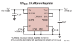
2A µModule Regulator Configurable as a Step-Down or an Inverter Is Safe up to 60VIN
The LTM8050 is a 2A µModule regulator that is protected against input surges up to 60V and can be configured as a step-down or an inverting (i.e., negative output) converter. With 60V input voltage protection, the LTM8050 can be used safely in applications where the main power bus may be susceptible to large voltage spikes or deviations. Examples of such applications are automotive, avionics, factory automation, heavy equipment, transportation, robotics and industrial systems.The operating input voltage of this device is from 3.6V to 58V (60Vmax) and the output is adjustable with one resistor from 0.8V to 24V. When configured as an inverter, the output is adjustable from -0.8V to -24V. The LTM8050 includes an inductor, DC/DC regulator, power FETs, and the compensation circuitry, all housed in a 9 x 15 x 4.92mm BGA package.To increase load current above 2A, up to four LTM8050s can be current shared to deliver as much as 8A. In systems sensitive to switching regulator noise requiring out of band operation, the LTM8050's switching frequency can be adjusted over a wide range from 100kHz to 2.4MHz with an external resistor. The LTM8050 is available for operation in two temperature ranges of -40°C to 125°C and -55°C and 125°C. 1000-piece pricing starts at $14.00 each.Request a Quote Supplied by Analog Devices Ltd -
LT3471 - Dual 1.3A, 1.2MHz Boost/Inverter in 3mm × 3mm DFN
The LT3471 dual switching regulator combines two 42V, 1.3A switches with error amplifiers that can sense to ground providing boost and inverting capability. The low VCESAT bipolar switches enable the device to deliver high current outputs in a small footprint. The LT3471 switches at 1.2MHz, allowing the use of tiny, low cost and low profile inductors and capacitors. High inrush current at start-up is eliminated using the programmable soft-start function, where an external RC sets the current ramp rate. A constant frequency current mode PWM architecture results in low, predictable output noise that is easy to filter. The LT3471 switches are rated at 42V, making the device ideal for boost converters up to ±40V as well as SEPIC and flyback designs. Each channel can generate 5V at up to 630mA from a 3.3V supply, or 5V at 510mA from four alkaline cells in a SEPIC design. The device can be configured as two boosts, a boost and inverter or two inverters. The LT3471 is available in a low profile (0.75mm) 10-lead 3mm × 3mm DFN package.Request a Quote Supplied by Analog Devices Ltd -
LT3587 - High Voltage Monolithic Inverter and Dual Boost
The LT3587 provides a one-chip solution for applications requiring two positive and one negative high voltage supplies.The LT3587 input voltage range of 2.5V to 6V makes it ideal for various battery-powered systems. A single resistor programs each of the three output voltage levels and the output current of Boost3. The intelligent softstart allows for sequential soft-start of the Boost1 output followed by the negative output with a single capacitor. Internal sequencing circuitry also disables the inverter until the Boost1 output has reached 87% of its final value. The LT3587 integrates all the power switches, soft-start, and output-disconnect circuits into a small 3mm x 3mm QFN package. This high level of integration combined with small external components makes the LT3587 ideal for space constrained applications.Request a Quote Supplied by Analog Devices Ltd -
LTC1261L - Switched Capacitor Regulated Voltage Inverter
The LTC1261L is a switched-capacitor voltage inverter designed to provide a regulated negative voltage from a single positive supply. The LTC1261L operates from a single 2.7V to 5.25V supply and provides an adjustable output voltage from -1.23V to ±5V. The LTC1261L-4/LTC1261L-4.5 needs a single 4.5V to 5.25V supply and provides a fixed output voltage of -4V to -4.5V respectively. Three external capacitors are required: a 0.1µF flying capacitor and an input and output bypass capacitors. An optional compensation capacitor at ADJ (COMP) can be used to reduce the output voltage ripple. Each version of the LTC1261L will supply up to 20mA output current with guaranteed output regulation of ±3.5%. The LTC1261L includes an open-drain REG output that pulls low when the output is within 5% of the set value. Quiescent current is typically 650µA when operating and 5µA in shutdown. The LTC1261L is available in 8-pin MSOP and SO packages.Request a Quote Supplied by Analog Devices Ltd -
LTC1261 - Switched Capacitor Regulated Voltage Inverter
The LTC1261 is a switched-capacitor voltage inverter designed to provide a regulated negative voltage from a single positive supply. The LTC1261CS operates from a single 3V to 8V supply and provides an adjustable output voltage from -1.25V to -8V. An on-chip resistor string allows the LTC1261CS to be configured for output voltages of -3.5V, -4V, -4.5V or -5V with no external components. The LTC1261CS8 is optimized for applications which use a 5V or higher supply or which require low output voltages. It requires a single external 0.1µF capacitor and provides adjustable and fixed output voltage options in 8-pin SO packages. The LTC1261CS requires one or two external 0.1µF capacitors, depending on input voltage. Both versions require additional external input and output bypass capacitors. An optional compensation capacitor at ADJ/COMP can be used to reduce the output voltage ripple. Each version of the LTC1261 will supply up to 12mA output current with guaranteed output regulation of 5%. The LTC1261 includes an open-drain REG output which pulls low when the output is within 5% of the set value. Output ripple is typically as low as 5mV. Quiescent current is typically 600µA when operating and 5µA in shutdown. The LTC1261 is available in a 14-pin narrow body SO package and an 8-pin SO package.Request a Quote Supplied by Analog Devices Ltd -
LTC1429 - Clock-Synchronized Switched Capacitor Regulated Voltage Inverter
Obsolete - Datasheet For Information Purposes Only. Contact Linear Technology for Potential Replacement The LTC®1429 is a switched-capacitor voltage inverter designed to provide a regulated negative voltage from a single positive supply and permits clock synchronization in noise sensitive systems. The LTC1429CS operates from a single 3V to 8V supply and provides an adjustable output voltage from -1.25V to -8V. An on-chip resistor string allows the LTC1429CS to be configured for output voltages of -3.5V, -4V,-4.5V or -5V. The LTC1429CS8 is optimized for applications which require a fixed -4V output from a 5V supply and requires only a single external 0.1µF flying capacitor. The LTC1429CS requires one or two external 0.1µF capacitors, depending on input voltage. Both versions require additional external input and output bypass capacitors. An optional compensation capacitor at ADJ/COMP can be used to reduce the output voltage ripple. Each version of the LTC1429 guarantees output regulation of 5%. The LTC1429 includes an open-drain REG output which pulls low when the output is within 5% of the set value. Output ripple is typically as low as 5mV. The LTC1429 requires an external clock applied to the SYNC/SD for normal operation and consumes a typical quiescent current of 600µA. Holding the SYNC/SD either high or low brings the device into shutdown and the supply current drops to 0.2µA. For applications which don't have a clock signal available, the LTC1261 provides the same functionality with an internal oscillator. For applications which require output ripple below 1mV, see the LTC1550/LTC1551. The LTC1429CS is available in a 14-pin SO package and the LTC1429CS8 is available in an 8-pin SO package.Request a Quote Supplied by Analog Devices Ltd -
LTC1550L - Low Noise, Switched Capacitor Regulated Voltage Inverters
The LTC1550L/LTC1551L are switched capacitor charge pump voltage inverters which include internal linear post-regulators to minimize output ripple. The LTC1550L fixed output voltage versions include ±4.1V, ±2.5V and ±2V with ripple voltages typically below 1mVP-P. The LTC1550L is also available in an adjustable output voltage version. The LTC1550L/LTC1551L are ideal for use as bias voltage generators for GaAs transmitter FETs in portable RF and cellular telephone applications. The LTC1550L/LTC1551L operate from single 2.7V to 5.5V supplies and draw typical quiescent currents of 3.5mA with a 5V supply. Each device includes a TTL compatible Shutdown pin which drops supply current to 0.2µA typically. The LTC1550L Shutdown pin is active low (SHDN), while the LTC1551L Shutdown pin is active high (SHDN). Only four external components are required: an input bypass capacitor, two 0.1µF charge pump capacitors and a filter capacitor at the linear regulator output. The adjustable LTC1550L/LTC1551L require two additional resistors to set the output voltage. The LTC1550L/LTC1551L will supply up to 20mA (depending on VCC to VOUT range), while maintaining guaranteed output regulation of ±2.5%. Both fixed voltage and adjustable LTC1550L/LTC1551L are available in 8-lead MSOP and SO plastic packages: the adjustable LTC1550L is also available in a 16-pin SSOP with the REG pin.Request a Quote Supplied by Analog Devices Ltd -
LTC1550 - Low Noise, Switched Capacitor-Regulated Voltage Inverters
The LTC1550/LTC1551 are switched capacitor charge pump voltage inverters which include internal linear post-regulators to minimize output ripple. Output voltages are fixed at -4.1V, with ripple voltages typically below 1mVP-P. The LTC1550 is also available in an adjustable output voltage version. The LTC1550/LTC1551 are ideal for use as bias voltage generators for GaAs transmitter FETs in portable RF and cellular telephone applications. The LTC1550/LTC1551 operate from single 4.5V to 6.5V supplies and draw typical quiescent currents of 4.25mA with a 5V supply. Each device includes a TTL compatible Shutdown pin which drops supply current to 0.2µA typically. The LTC1550 Shutdown pin is active low (SHDN), while the LTC1551 Shutdown pin is active high (SHDN). Only four external components are required: an input bypass capacitor, two 0.1µF charge pump capacitors and a filter capacitor at the linear regulator output. The adjustable LTC1550 requires two additional resistors to set the output voltage. The LTC1550/LTC1551 will supply up to 10mA output current with a 5V supply, while maintaining guaranteed output regulation of ±5%. The fixed voltage LTC1550/LTC1551 are available in S0-8 plastic packages. The adjustable LTC1550 is available in a 16-pin SSOP.Request a Quote Supplied by Analog Devices Ltd -
LTC1551L - Low Noise, Switched Capacitor Regulated Voltage Inverters
The LTC1550L/LTC1551L are switched capacitor charge pump voltage inverters which include internal linear post-regulators to minimize output ripple. The LTC1550L fixed output voltage versions include ±4.1V, ±2.5V and ±2V with ripple voltages typically below 1mVP-P. The LTC1550L is also available in an adjustable output voltage version. The LTC1550L/LTC1551L are ideal for use as bias voltage generators for GaAs transmitter FETs in portable RF and cellular telephone applications. The LTC1550L/LTC1551L operate from single 2.7V to 5.5V supplies and draw typical quiescent currents of 3.5mA with a 5V supply. Each device includes a TTL compatible Shutdown pin which drops supply current to 0.2µA typically. The LTC1550L Shutdown pin is active low (SHDN), while the LTC1551L Shutdown pin is active high (SHDN). Only four external components are required: an input bypass capacitor, two 0.1µF charge pump capacitors and a filter capacitor at the linear regulator output. The adjustable LTC1550L/LTC1551L require two additional resistors to set the output voltage. The LTC1550L/LTC1551L will supply up to 20mA (depending on VCC to VOUT range), while maintaining guaranteed output regulation of ±2.5%. Both fixed voltage and adjustable LTC1550L/LTC1551L are available in 8-lead MSOP and SO plastic packages: the adjustable LTC1550L is also available in a 16-pin SSOP with the REG pin.Request a Quote Supplied by Analog Devices Ltd -
LTC1551 - Low Noise, Switched Capacitor-Regulated Voltage Inverters
The LTC1550/LTC1551 are switched capacitor charge pump voltage inverters which include internal linear post-regulators to minimize output ripple. Output voltages are fixed at -4.1V, with ripple voltages typically below 1mVP-P. The LTC1550 is also available in an adjustable output voltage version. The LTC1550/LTC1551 are ideal for use as bias voltage generators for GaAs transmitter FETs in portable RF and cellular telephone applications. The LTC1550/LTC1551 operate from single 4.5V to 6.5V supplies and draw typical quiescent currents of 4.25mA with a 5V supply. Each device includes a TTL compatible Shutdown pin which drops supply current to 0.2µA typically. The LTC1550 Shutdown pin is active low (SHDN), while the LTC1551 Shutdown pin is active high (SHDN). Only four external components are required: an input bypass capacitor, two 0.1µF charge pump capacitors and a filter capacitor at the linear regulator output. The adjustable LTC1550 requires two additional resistors to set the output voltage. The LTC1550/LTC1551 will supply up to 10mA output current with a 5V supply, while maintaining guaranteed output regulation of ±5%. The fixed voltage LTC1550/LTC1551 are available in S0-8 plastic packages. The adjustable LTC1550 is available in a 16-pin SSOP.Request a Quote Supplied by Analog Devices Ltd