
Analog Devices Ltd
Analog Devices, Inc. operates at the centre of the modern digital economy, converting real-world phenomena into actionable insight with its comprehensive suite of analogue and mixed signal, power management, radio frequency (RF), and digital and sensor technologies. ADI serves 125,000 customers worldwide with more than 75,000 products in the industrial, communications, automotive, and consumer markets. ADI is headquartered in Wilmington, MA. Visit www.analog.com. Both Linear Technology and Maxim Integrated are now part of Analog Devices.
Analog Devices provide efficient solutions for power management and power conversion applications in the automotive, telecommunications, industrial, medical, computing, military and high-end consumer markets using high-performance analogue ICs. Our power ICs can provide unrivalled power densities and software design simulation tools to provide both fast and accurate power module and power supply designs.
Products for power management include: switching regulators, linear regulators (LDO), µModule regulators, PMIC & Multifunction, inductorless (charge pump) DC/DC converters, LED driver ICs, power control, battery management, current source, system supervisor, hot-swap controllers, monitor and control, energy harvesting, super capacitor chargers and power management evaluation kits.
Filter products and services
-
LTC1065 - DC Accurate, Clock-Tunable Linear Phase 5th Order Bessel Lowpass Filter
The LTC1065 is the first monolithic filter providing both clock-tunability with low DC output offset and over 12-bit DC accuracy. The frequency response of the LTC1065 closely approximates a 5th order Bessel polynomial. With appropriate PCB layout techniques the output DC offset is typically 1mV and is constant over a wide range of clock frequencies. With ±5V supplies and ±4V input voltage range, the CMR of the device is typically 80dB.The filter cutoff frequency is controlled either by an internal or external clock. The clock-to-cutoff frequency ratio is 100:1. The on-board clock is nearly power supply independent and it is programmed via an external RC. The 50µVRMS clock feedthrough of the device is considerably lower than other existing monolithic filters.The LTC1065 wideband noise is 80µVRMS and it can process large AC input signals with low distortion. With ±7.5V supplies, for instance, the filter handles up to 4VRMS (94dB S/N ratio) while the standard 1kHz THD is below 0.005%; 87dB dynamic range (S/N THD) is obtained with input levels between 2VRMS and 2.5VRMS.The LTC1065 is available in 8-pin miniDIP and 16-pin SOL. For a Butterworth response, see LTC1063 data sheet. The LTC1065 is pin compatible with the LTC1063.Request a Quote Supplied by Analog Devices Ltd -
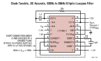
LTC1066-1 - 14-Bit DC Accurate Clock-Tunable, 8th Order Elliptic or Linear Phase Lowpass Filter
The LTC1066-1 is an 8th order elliptic lowpass filter which simultaneously provides clock-tunability and DC accuracy. The unique and proprietary architecture of the filter allows 14 bits of DC gain linearity and a maximum of 1.5mV DC offset. An external RC is required for DC accurate operation. With ±7.5V supplies, a 20k resistor and a 1µF capacitor, the cutoff frequency can be tuned from 800Hz to 100kHz. A clock-tunable 10Hz to 100kHz operation can also be achieved (see Typical Application section).The filter does not require any external active components such as input/output buffers. The input/output impedance is 500Mohms/0.1ohms and the output of the filter can source or sink 40mA. When pin 8 is connected to V +, the clock-to-cutoff frequency ratio is 50:1 and the input signal is sampled twice per clock cycle to lower the risk of aliasing. For frequencies up to 0.75fCUTOFF, the passband ripple is µ0.15dB. The gain at fCUTOFF is -1dB and the filter's stopband attenuation is 80dB at 2.3fCUTOFF. Linear phase operation is also available with a clock-to-cutoff frequency ratio of 100:1 when pin 8 is connected to ground.The LTC1066-1 is available in an 18-pin SO Wide package..Request a Quote Supplied by Analog Devices Ltd -
LTC1067 - Rail-to-Rail, Very Low Noise Universal Dual Filter Building Block
The LTC®1067/LTC1067-50 consist of two identical rail-to-rail, high accuracy and very wide dynamic range 2nd order switched-capacitor building blocks. Each building block, together with three to five resistors, provides 2nd order filter functions such as bandpass, highpass, lowpass, notch and allpass. High precision 4th order filters are easily designed. The center frequency of each 2nd order section is tuned by the external clock frequency. The internal clock-to-center frequency ratio (100:1 for the LTC1067 and 50:1 for the LTC1067-50) can be modified by the external resistors. These devices have a double sampled architecture which places aliasing and imaging components at twice the clock frequency. The LTC1067-50 is a low power device consuming about one half the current of the LTC1067. The LTC1067-50's typical supply current is about 1mA from a 3.3V supply. The LTC1067 and LTC1067-50 are available in 16-pin narrow SSOP and SO packages. Mask programmable versions of the LTC1067 and LTC1067-50, with thin film resistors on-chip and custom clock-to-cutoff frequency ratios, can be designed in an SO-8 package to realize application specific monolithic filters. Please contact LTC Marketing for more details.Request a Quote Supplied by Analog Devices Ltd -
LTC1068 - Clock-Tunable, Quad Second Order, Filter Building Blocks
The LTC1068 product family consists of four monolithic clock-tunable filter building blocks. Each product contains four matched, low noise, high accuracy 2nd order switched-capacitor filter sections. An external clock tunes the center frequency of each 2nd order filter section. The LTC1068 products differ only in their clock-to-center frequency ratio. The clock-to-center frequency ratio is set to 200:1 (LTC1068-200), 100:1 (LTC1068), 50:1 (LTC1068-50) or 25:1 (LTC1068-25). External resistors can modify the clock-to-center frequency ratio. High performance, quad 2nd order, dual 4th order or 8th order filters can be designed with an LTC1068 family product. Designing filters with an LTC1068 product is fully supported by FilterCAD™ filter design software for Windows®. The LTC1068 products are available in a 28-pin SSOP surface mount package. A customized version of an LTC1068 family product can be obtained in a 16-lead SO package with internal thin-film resistors. Please contact LTC Marketing for details.Request a Quote Supplied by Analog Devices Ltd -
LTC1069-1 - Low Power, 8th Order Progressive Elliptic, Lowpass Filter
The LTC®1069-1 is a monolithic 8th order lowpass filter featuring clock-tunable cutoff frequency and 2.5mA power supply current with a single 5V supply. An additional feature of the LTC1069-1 is operation with a single 3.3V supply. The cutoff frequency (fCUTOFF) of the LTC1069-1 is equal to the clock frequency divided by 100. The gain at fCUTOFFM is -0.7dB and the typical passband ripple is ±0.15dB up to 0.9fCUTOFF. The stopband attenuation of the LTC1069-1 features a progressive elliptic response reaching 20dB attenuation at 1.2fCUTOFF, 52dB attenuation at 1.4fCUTOFF and 70dB attenuation at 2fCUTOFF. With ±5V supplies, the LTC1069-1 cutoff frequency can be clock-tuned up to 12kHz; with a single 5V supply, the maximum cutoff frequency is 8kHz. The low power feature of the LTC1069-1 does not penalize the device's dynamic range. With ±5V supplies and an input range of 0.3VRMS to 2.5VRMS, the signal-to-(noise + THD) ratio is ≥70dB. The wideband noise of the LTC1069-1 is 110ΜVRMS. Other filter responses with lower power or higher speed can be obtained. Please contact LTC marketing for details. The LTC1069-1 is available in 8-pin PDIP and 8-pin SO packages.Request a Quote Supplied by Analog Devices Ltd -
LTC1069-6 - Single Supply, Very Low Power, Elliptic Lowpass Filter
The LTC1069-6 is a monolithic low power, 8th order lowpass filter optimized for single 3V or single 5V supply operation. The LTC1069-6 typically consumes 1mA under single 3V supply operation and 1.2mA under 5V operation. The cutoff frequency of the LTC1069-6 is clock tunable and it is equal to the clock frequency divided by 50. The input signal is sampled twice per clock cycle to lower the risk of aliasing. The typical passband ripple is ± 0.1dB up to 0.9fCUTOFF. The gain at fCUTOFF is -0.7dB. The transition band of the LTC1069-6 features progressive attenuation reaching 42dB at 1.3fCUTOFF and 70dB at 2.1fCUTOFF. The maximum stopband attenuation is 72dB. The LTC1069-6 can be clock tuned for cutoff frequencies up to 20kHz (single 5V supply) and for cutoff frequencies up to 14kHz (single 3V supply). The low power feature of the LTC1069-6 does not penalize the device's dynamic range. With single 5V supply and an input range of 0.4VRMS to 1.4VRMS, the Signal-to- (Noise + THD) ratio is ≥70dB. The wideband noise of the LTC1069-6 is 125ΜVRMS. Other filter responses with higher speed can be obtained. Please contact LTC Marketing for details. The LTC1069-6 is available in an 8-pin SO package.Request a Quote Supplied by Analog Devices Ltd -
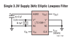
LTC1069-7 - Linear Phase 8th Order Lowpass Filter
The LTC®1069-7 is a monolithic, clock-tunable, linear phase, 8th order lowpass filter. The amplitude response of the filter approximates a raised cosine filter with an alpha of one. The gain at the cutoff frequency is -3dB and the attenuation at twice the cutoff frequency is 43dB. The cutoff frequency of the LTC1069-7 is set by an external clock and is equal to the clock frequency divided by 25. The ratio of the internal sampling frequency to the cutoff frequency is 50:1 that is, the input signal is sampled twice per clock cycle to lower the risk of aliasing. The LTC1069-7 can be operated from a single 5V supply up to dual ±5V supplies. The gain and phase response of the LTC1069-7 can be used in digital communication systems where pulse shaping and channel bandwidth limiting must be carried out. Any system that requires an analog filter with linear phase and sharper roll off than conventional Bessel filters can use the LTC1069-7. The LTC1069-7 has a wide dynamic range. With ±5V supplies and an input range of 0.1VRMS to 2VRMS, the signal-to-(noise + THD) ratio is ≥ 60dB. The wideband noise of the LTC1069-7 is 140ΜVRMS. Unlike other LTC1069-X filters,> the typical passband gain of the LTC1069-7 is equal to -1V/V. The LTC1069-7 is available in an SO-8 package. Other filter responses with lower power/speed specifications can be obtained. Please contact LTC Marketing.Request a Quote Supplied by Analog Devices Ltd -
LTC1090 - Single Chip 10-Bit Data Acquisition System
The LTC™1090 is a data acquisition component which contains a serial I/O successive approximation A/D converter. It uses LTCMOS® switched capacitor technology to perform either 10-bit unipolar, or 9-bit plus sign bipolar A/D conversions. The 8-channel input multiplexer can be configured for either single ended or differential inputs (or combinations thereof). An on-chip sample and hold is included for all single ended input channels. The serial I/O is designed to be compatible with industry standard full duplex serial interfaces. It allows either MSB or LSB first data and automatically provides 2's complement output coding in the bipolar mode. The output data word can be programmed for a length of 8, 10, 12 or 16 bits. This allows easy interface to shift registers and a variety of processors. The LTC1090A is specified with total unadjusted error (including the effects of offset, linearity and gain errors) less than ?0.5LSB. The LTC1090 is specified with offset and linearity less than ?0.5LSB but with a gain error limit of ?2LSB for applications where gain is adjustable or less critical.Request a Quote Supplied by Analog Devices Ltd -
LTC1091 - 1, 2, 6 and 8 Channel, 10-Bit Serial I/O Data Acquisition Systems
The high impedance analog inputs and the ability to operate with reduced spans (below 1V full scale) allow direct connection to sensors and transducers in many applications, eliminating the need for gain stages. An efficient serial port communicates without external hardware to most MPU serial ports and all MPU parallel I/O ports allowing eight channels of data to be transmitted over as few as three wires. This, coupled with low power consumption, makes remote location possible and facilitates transmitting data through isolation barriers. Temperature drift of offset, linearity and full-scale error are all extremely low (1ppm/°C typically) allowing all grades to be specified with offset and linearity errors of ±0.5LSB maximum over temperature. In addition, the A grade devices are specified with full-scale error and total unadjusted error (including the effects of offset, linearity and full-scale errors) of ±1LSB maximum over temperature. The lower grade has a full-scale specification of ±2LSB for applications where full scale is adjustable or less critical.Request a Quote Supplied by Analog Devices Ltd -
LTC1092 - 1, 2, 6 and 8 Channel, 10-Bit Serial I/O Data Acquisition Systems
The high impedance analog inputs and the ability to operate with reduced spans (below 1V full scale) allow direct connection to sensors and transducers in many applications, eliminating the need for gain stages. An efficient serial port communicates without external hardware to most MPU serial ports and all MPU parallel I/O ports allowing eight channels of data to be transmitted over as few as three wires. This, coupled with low power consumption, makes remote location possible and facilitates transmitting data through isolation barriers. Temperature drift of offset, linearity and full-scale error are all extremely low (1ppm/°C typically) allowing all grades to be specified with offset and linearity errors of ±0.5LSB maximum over temperature. In addition, the A grade devices are specified with full-scale error and total unadjusted error (including the effects of offset, linearity and full-scale errors) of ±1LSB maximum over temperature. The lower grade has a full-scale specification of ±2LSB for applications where full scale is adjustable or less critical.Request a Quote Supplied by Analog Devices Ltd