
Analog Devices Ltd
Analog Devices, Inc. operates at the centre of the modern digital economy, converting real-world phenomena into actionable insight with its comprehensive suite of analogue and mixed signal, power management, radio frequency (RF), and digital and sensor technologies. ADI serves 125,000 customers worldwide with more than 75,000 products in the industrial, communications, automotive, and consumer markets. ADI is headquartered in Wilmington, MA. Visit www.analog.com. Both Linear Technology and Maxim Integrated are now part of Analog Devices.
Analog Devices provide efficient solutions for power management and power conversion applications in the automotive, telecommunications, industrial, medical, computing, military and high-end consumer markets using high-performance analogue ICs. Our power ICs can provide unrivalled power densities and software design simulation tools to provide both fast and accurate power module and power supply designs.
Products for power management include: switching regulators, linear regulators (LDO), µModule regulators, PMIC & Multifunction, inductorless (charge pump) DC/DC converters, LED driver ICs, power control, battery management, current source, system supervisor, hot-swap controllers, monitor and control, energy harvesting, super capacitor chargers and power management evaluation kits.
Filter products and services
-
LT3484 - Photoflash Capacitor Charger
The LT3484 family of photoflash capacitor charger ICs is designed for use in digital camera and mobile phone applications where space is at a premium. The LT3484's patented control technique allows it to use extremely small transformers, and the improved NPN power switch requires no external Schottky diode clamp, reducing solution size. Output voltage detection requires no external circuitry as the transformer turns ratio determines final charge voltage. The devices feature a VBAT pin, which allows the use of 2 alkaline cells to charge the capacitor. The LT3484-0, -2 and -1 have primary current limits of 1.4A, 1A and 0.7A respectively, resulting in tightly controlled average input current of 500mA, 350mA and 225mA respectively. The three versions are otherwise identical. The CHARGE pin gives full control of the part to the user. Driving CHARGE low puts the part in shutdown. The DONE pin indicates when the part has completed charging. The LT3484 series of parts are housed in a tiny low profile 2mm × 3mm DFN package.Request a Quote Supplied by Analog Devices Ltd -
LT3485 - Photoflash Capacitor Chargers with Output Voltage Monitor and Integrated IGBT Drive
The LT3485 family of photoflash chargers are highly integrated ICs containing complete charger and IGBT drive functions. The patented control technique of the LT3485-x allows it to use extremely small transformers. Output voltage detection requires no external circuitry. The turns ratio of the transformer controls the final charge voltage. While charging, the output voltage on the capacitor may be monitored by a microcontroller from the monitor pin. Each device contains an on-chip high voltage NPN power switch, which can withstand negative voltages on the switch pin without an external Schottky diode. The device features a VBAT pin, which allows the use of two AA cells to charge the capacitor. The internal circuitry operates from the VIN pin. The LT3485-0 has a primary current limit of 1.4A, whereas the LT3485-3, LT3485-2, and LT3485-1 have current limits of 2A, 1A and 0.7A respectively. These different current limits result in tightly controlled input currents. The CHARGE pin gives full control of the part to the user. Driving CHARGE low puts the part in shutdown. The DONE pin indicates when the part has completed charging. The LT3485 series of parts are housed in a leadless (3mm × 3mm) DFN package.Request a Quote Supplied by Analog Devices Ltd -
LT3750 - Capacitor Charger Controller
The LT3750 is a flyback converter designed to rapidly charge large capacitors to a user-adjustable target voltage. A patented boundary mode control scheme* minimizes transition losses and reduces transformer size. The transformer turns ratio and two external resistors easily adjust the output voltage. A low 78mV current sense accurately limits peak switch current and also helps to maximize efficiency. With a wide input voltage range, the LT3750 can operate from a variety of power sources. A typical application can charge a 100ΜF capacitor to 300V in less than 300ms. The CHARGE pin gives full control of the LT3750 to the user. The DONE pin indicates when the capacitor has reached its programmed value and the part has stopped charging.Request a Quote Supplied by Analog Devices Ltd -
LT3751 - High Voltage Capacitor Charger Controller with Regulation
The LT3751 is a high input voltage capable flyback controller designed to rapidly charge a large capacitor to a user-adjustable high target voltage set by the transformer turns ratio and three external resistors. Optionally, a feedback pin can be used to provide a low noise high voltage regulated output. The LT3751 has an integrated rail-to-rail MOSFET gate driver that allows for efficient operation down to 4.75V. A low 106mV differential current sense threshold voltage accurately limits the peak switch current. Added protection is provided via user-selectable overvoltage and undervoltage lockouts for both VCC and VTRANS. A typical application can charge a 1000ΜF capacitor to 500V in less than one second. The CHARGE pin is used to initiate a new charge cycle and provides ON/OFF control. The DONE pin indicates when the capacitor has reached its programmed value and the part has stopped charging. The FAULT pin indicates when the LT3751 has shut down due to either VCC or VTRANS voltage exceeding the user-programmed supply tolerances.Request a Quote Supplied by Analog Devices Ltd -
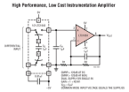
LTC1043 - Dual Precision Instrumentation Switched-Capacitor Building Block
The LTC™1043 is a monolithic, charge-balanced, dual switched capacitor instrumentation building block. A pair of switches alternately connects an external capacitor to an input voltage and then connects the charged capacitor across an output port. The internal switches have a break-before-make action. An internal clock is provided and its frequency can be adjusted with an external capacitor.The LTC1043 can also be driven with an external CMOS clock. The LTC1043, when used with low clock frequencies, provides ultra precision DC functions without requiring precise external components. Such functions are differential voltage to single-ended conversion, voltage inversion, voltage multiplication and division by 2, 3, 4, 5, etc. The LTC1043 can also be used for precise VµF and FµV circuits without trimming, and it is also a building block for switched capacitor filters, oscillators and modulators. The LTC1043 is manufactured using Linear Technology's enhanced LTCMOS® silicon gate process.Request a Quote Supplied by Analog Devices Ltd -
LTC1047 - Dual Micropower Zero-Drift Operational Amplifier with Internal Capacitors
The LTC®1047 is a micropower, high performance dual zero-drift operational amplifier. The sample-and-hold capacitors usually required by other chopper amplifiers are integrated on-chip, minimizing the need for external components.The LTC1047 has a typical offset voltage of 3µV, drift of 10nV/°C, input noise voltage typically 3.5µVP-P, and typical voltage gain of 150dB. The common mode rejection is 110dB minimum, with minimum power supply rejection of 105dB. The LTC1047 also offers a 0.2V/µs slew rate and a gain bandwidth product of 200kHz. Overload recovery time from saturation is 70ms, four times faster than chopper amplifiers with external capacitors.The LTC1047 is available in a standard plastic 8-pin PDIP as well as a 16-pin SW package. The LTC1047 is a plug-in replacement for most dual op amps with improved DC performance and substantial power savings.Request a Quote Supplied by Analog Devices Ltd -
LTC1049 - Low Power Zero-Drift Operational Amplifier with Internal Capacitors
The LTC1049 is a high performance, low power zero-drift operational amplifier. The two sample-and-hold capacitors usually required externally by other chopper stabilized amplifiers are integrated on the chip. Further, the LTC1049 offers superior DC and AC performance with a nominal supply current of only 200µA.The LTC1049 has a typical offset voltage of 2µV, drift of 0.02µV/°C, 0.1Hz to 10Hz input noise voltage of 3µVP-P and typical voltage gain of 160dB. The slew rate is 0.8V/µs with a gain bandwidth product of 0.8MHz.Overload recovery time from a saturation condition is 6ms, a significant improvement over chopper amplifiers using external capacitors.The LTC1049 is available in a standard 8-pin plastic dual in line, as well as an 8-pin SO package. The LTC1049 can be a plug-in replacement for most standard op amps with improved DC performance and substantial power savings.Request a Quote Supplied by Analog Devices Ltd -
LTC1050 - Precision Zero-Drift Operational Amplifier with Internal Capacitors
The LTC®1050 is a high performance, low cost zero-drift operational amplifier. The unique achievement of the LTC1050 is that it integrates on-chip the two sample-and-hold capacitors usually required externally by other chopper amplifiers. Further, the LTC1050 offers better combined overall DC and AC performance than is available from other chopper stabilized amplifiers with or without internal sample-and-hold capacitors.The LTC1050 has an offset voltage of 0.5µV, drift of 0.01µV/°C, DC to 10Hz, input noise voltage of 1.6µVP-P and a typical voltage gain of 160dB. The slew rate of 4V/µs and a gain bandwidth product of 2.5MHz are achieved with only 1mA of supply current.Overload recovery times from positive and negative saturation conditions are 1.5ms and 3ms respectively, which represents an improvement of about 100 times over chopper amplifiers using external capacitors. Pin 5 is an optional external clock input, useful for synchronization purposes.The LTC1050 is available in standard 8-pin metal can, plastic and ceramic dual-in-line packages as well as an SO-8 package. The LTC1050 can be an improved plug-in replacement for most standard op amps.Request a Quote Supplied by Analog Devices Ltd -
LTC1051 - Dual/Quad Precision Zero-Drift Operational Amplifiers With Internal Capacitors
The LTC®1051/LTC1053 are high performance, low cost dual/quad zero-drift operational amplifiers. The unique achievement of the LTC1051/LTC1053 is that they integrate on chip the sample-and-hold capacitors usually required externally by other chopper amplifiers. Further, the LTC1051/LTC1053 offer better combined overall DC and AC performance than is available from other chopper stabilized amplifiers with or without internal sample/hold capacitors.The LTC1051/LTC1053 have an offset voltage of 0.5µV, drift of 0.01µV/°C, DC to 10Hz, input noise voltage typically 1.5µVP-P and typical voltage gain of 140dB. The slew rate of 4V/µs and gain bandwidth product of 2.5MHz are achieved with only 1mA of supply current per op amp.Overload recover times from positive and negative saturation conditions are 1.5ms and 3ms respectively, about a 100 or more times improvement over chopper amplifiers using external capacitors.The LTC1051 is available in an 8-lead standard plastic dual-in-line package as well as a 16-pin SW package. The LTC1053 is available in a standard 14-pin plastic package and an 18-pin SO. The LTC1051/LTC1053 are plug in replacements for most standard dual/quad op amps with improved performance.Request a Quote Supplied by Analog Devices Ltd -
LTC1053 - Dual/Quad Precision Zero-Drift Operational Amplifiers With Internal Capacitors
The LTC®1051/LTC1053 are high performance, low cost dual/quad zero-drift operational amplifiers. The unique achievement of the LTC1051/LTC1053 is that they integrate on chip the sample-and-hold capacitors usually required externally by other chopper amplifiers. Further, the LTC1051/LTC1053 offer better combined overall DC and AC performance than is available from other chopper stabilized amplifiers with or without internal sample/hold capacitors.The LTC1051/LTC1053 have an offset voltage of 0.5µV, drift of 0.01µV/°C, DC to 10Hz, input noise voltage typically 1.5µVP-P and typical voltage gain of 140dB. The slew rate of 4V/µs and gain bandwidth product of 2.5MHz are achieved with only 1mA of supply current per op amp.Overload recover times from positive and negative saturation conditions are 1.5ms and 3ms respectively, about a 100 or more times improvement over chopper amplifiers using external capacitors.The LTC1051 is available in an 8-lead standard plastic dual-in-line package as well as a 16-pin SW package. The LTC1053 is available in a standard 14-pin plastic package and an 18-pin SO. The LTC1051/LTC1053 are plug in replacements for most standard dual/quad op amps with improved performance.Request a Quote Supplied by Analog Devices Ltd