


Analog Devices Ltd
Analog Devices, Inc. operates at the centre of the modern digital economy, converting real-world phenomena into actionable insight with its comprehensive suite of analogue and mixed signal, power management, radio frequency (RF), and digital and sensor technologies. ADI serves 125,000 customers worldwide with more than 75,000 products in the industrial, communications, automotive, and consumer markets. ADI is headquartered in Wilmington, MA. Visit www.analog.com. Both Linear Technology and Maxim Integrated are now part of Analog Devices.
Analog Devices provide efficient solutions for power management and power conversion applications in the automotive, telecommunications, industrial, medical, computing, military and high-end consumer markets using high-performance analogue ICs. Our power ICs can provide unrivalled power densities and software design simulation tools to provide both fast and accurate power module and power supply designs.
Products for power management include: switching regulators, linear regulators (LDO), µModule regulators, PMIC & Multifunction, inductorless (charge pump) DC/DC converters, LED driver ICs, power control, battery management, current source, system supervisor, hot-swap controllers, monitor and control, energy harvesting, super capacitor chargers and power management evaluation kits.
Filter products and services
-
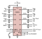
Complete Power Management IC Solutions for i.MX6, ARM Cortex & Other Advanced Portable Application Processor Systems
The LTC3676 and LTC3676-1 are complete PMIC power management solutions for portable processors including Freescale's i.MX6 series, PXA, OMAP, ARM Cortex and other advanced portable microprocessor-based systems. These devices contain four synchronous step-down DC/DC converters for core, memory, I/O and system on-chip (SoC) rails plus three 300mA low dropout (LDO) regulators for low noise analog supplies with dynamic control & sequencing. The LTC3676-1 configures a 1.5A buck regulator for source/sink and tracking operation to support DDR memory termination and also adds a VTTR reference output for DDR. These two pin features replace the LDO4 enable and feedback pins of the LTC3676. Supporting the multiple regulators is a highly configurable power sequencing capability, dynamic voltage scaling output voltage control, a pushbutton interface controller, plus regulator control via an I²C interface with extensive status reporting and an interrupt output.The LTC3676's four constant frequency current-mode buck switching regulators are internally compensated and provide up to 2.5A, 2.5A, 1.5A and 1.5A output currents, and have complete I²C-control, including selectable switching frequencies (2.25MHz or 1.125MHz) and phasing. The device's power-on default frequency is 2.25MHz with switch edge rate adjustment for reduced EMI. The LTC3676 also has four LDOs for low noise analog supplies, including three 300mA rails with different combinations of fixed and I2C-selectable voltage options; two of these regulators feature adjustable outputs the other is an always-on 25mA supply with a resistor-programmable output voltage.The LTC3676/-1 is available in a low profile (0.75mm) 40-pin 6mm × 6mm QFN package. 1000-piece pricing starts at $5.50 each. In addition to E-grade and I-grade there is the H-grade version which can operate from -40°C to +150°C.Request a Quote Supplied by Analog Devices Ltd -
Convert Any Input Voltage from 2.8V to 80V into a Fixed Output Voltage or Output Current with Up to 98% Efficiency at 250W
The LT8705 is a very high efficiency (up to 98%) synchronous buck-boost DC/DC controller that operates from input voltages above, below or equal to the regulated output voltage. This device has four feedback loops to regulate the input current/voltage, along with the output current/voltage. The input current and voltage feedback loops can prevent overloading of solar cells. The output current loop provides a regulated output current for a battery charger or current source. The LT8705 can be used in a wide range of applications such as a voltage stabilizer in telecom and automotive requirements, as well as in solar or high impedance sources and battery systems.This DC/DC controller operates over a wide 2.8V to 80V input voltage range and produces a 1.3V to 80V output, using a single inductor with 4-switch synchronous rectification. Output power up to 250W can be delivered with a single device. Higher output power can be achieved when multiple circuits are paralleled. The operating frequency is selectable between 100kHz and 400kHz, and can be synchronized to an external clock. The LT8705 employs a proprietary current-mode control architecture for constant frequency operation in buck or boost mode and has powerful onboard quad N-channel MOSFET gate drivers. The user can select among forced continuous, discontinuous and Burst Mode operation to maximize light load efficiency.Additional features include servo pins to indicate which feedback loops are active, a 3.3V/12mA LDO, adjustable soft-start, onboard die temperature monitor and ±1% reference voltage accuracy over an operating junction temperature range of -40°C to 125°C. The LT8705 is available in a 38-pin 5mm x 7mm QFN, and also a 38-lead TSSOP package with additional pin spacing for high voltage operation. Pricing starts at $5.95 each in 1,000-piece quantities.Request a Quote Supplied by Analog Devices Ltd -
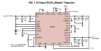
Dual 13A or Single 26A DC/DC µModule Step-Down Regulator with Integrated Heat Sink Delivers up to 100A
The LTM4620 is a dual 13A per output or single 26A output DC/DC µModule step-down regulator that delivers up to 100A when four devices are current shared. This device is a complete DC/DC regulator system in a 15mm x 15mm x 4.41mm LGA package, including inductors, power stages and all control circuits. For optimum heat dissipation, a patented top side heat sink removes heat quickly and evenly. With 200LFM air flow, 12VIN to 1.0VOUT and at full load of 26A (or 13A per output), the LTM4620 internal temperature rises only 60°C above ambient. With the addition of an external heat sink to the top of the package and 200LFM air flow, the temperature rise is only 40°C. The LTM4620 is designed to convert 5V to 12V inputs to high power, low voltage point-of-load system rails such as 2.5V to as low as 0.6V. An accurate reference and an internal remote sense amplifier guarantee +/-1.5% accurate output regulation over line, load and temperature. Sensing the voltage at the load compensates for voltage drops caused by PCB trace impedance. Excellent heat dissipation, low temperature rise, scalable and high output power capability, small footprint and the low profile package of the LTM4620 enable system designers to lay out more densely populated boards. Applications include mezzanine boards such as ATCA and microTCA systems, point-of-load regulation for advanced processors, ASICs and recently introduced 28nm FPGAs as well as high-speed SERDES.The LTM4620 features fast short-circuit protection where a current foldback technique reduces IOUT to a minimum, preventing the µModule regulator from overheating while protecting the load as well as the upstream power supply. Once the short-circuit condition is removed the LTM4620 resumes operation. The LTM4620 is rated for operation from -40°C to 125°C. 1,000-piece pricing starts at $29.99 each.Request a Quote Supplied by Analog Devices Ltd -
Dual 750mA/250mA Linear LDO Regulator with Independent Inputs Offers Ultralow Noise
The LT3030 is a dual low noise, low dropout regulator with independent inputs and independent shutdown control for each channel. It delivers continuous output current up to 750mA on one channel and 250mA on the other channel, with a low dropout voltage of only 300mV at full load. The LT3030 provides a wide 1.8V to 20V input voltage range, delivering output voltages as low as 1.215V and up to 19.5V. This low dropout regulator also features ultralow 20µVRMS noise across a wide 10Hz to 100kHz bandwidth, a precision shutdown/UVLO threshold for each channel, tracking/sequencing capability and dual PWRGD flags to indicate output regulation per channel. The LT3030's full feature set and low quiescent current of 115µA/70µA per regulator (operating) and <1µA each (in shutdown) make it ideal for battery-powered "keep alive" systems that require optimum run time, as well as microprocessor core logic supplies, tracking/sequencing supplies and general-purpose voltage conversion.The LT3030 operates with very small, low cost, ceramic output capacitors, optimizing stability and transient response. It is stable with only a 10µF ceramic output capacitor on the 750mA channel and a 3.3µF ceramic output capacitor on the 250mA channel. Internal protection circuitry includes reverse-battery, no reverse current flow from output to input, current limiting with foldback and thermal shutdown. The thermal shutdown circuitry protects both channels if an overload or fault condition occurs on either channel.The LT3030's compact packages are available in 20-lead thermally enhanced TSSOP and 28-lead 4mm x 5mm QFN packages in a wide variety of grades and temperature ranges. 1,000-piece pricing starts at $3.27.Request a Quote Supplied by Analog Devices Ltd -
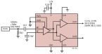
Dual Output Sine Wave to Logic Converter utilises Selectable Input Filtering for Lowest Additive Jitter
The LTC6957 is a DC to 300MHz dual output buffer/driver/logic translator, ideal for converting sine waves into low phase noise logic level signals.Prior solutions were unable to perform this conversion without introducing a significant amount of jitter. The LTC6957 converts any DC to 300MHz reference frequency into dual LVPECL, LVDS or CMOS outputs with exceptionally low additive jitter of 45fsRMS (LVPECL) over the 12kHz to 20MHz integration bandwidth and less than 200fsRMS total jitter.The device also features a proprietary, selectable, input stage bandwidth-limiting feature, which substantially improves the additive phase noise for slow slewing signals by 4-7dB.While the LTC6957 can be used to convert any signal type to a logic level signal, it particularly excels with sine waves. The selectable, band-limited input stage enables optimal conversion of sine waves with the lowest additive jitter.The device is ideal for systems that distribute system clock references for board level synchronization. It can also be used as a clock driver for analog-to-digital converters (ADCs), digital-to-analog converters (DACs) or DDS (direct digital synthesis) ICs with clock rates up to 300MHz.The LTC6957 is offered in four output logic signal types: the LTC6957-1 provides two LVPECL outputs, the LTC6957-2 provides two LVDS logic outputs, and the LTC6957-3 and LTC6957-4 offer two in-phase CMOS or complementary CMOS outputs, respectively, with output skew as low as 3ps (typ).Each device is available in small RoHS-compliant 12-pin MSOP or 3mm x 3mm DFN packages and can be ordered in industrial and automotive grades, supporting operating temperature ranges from -40°C to 85°C and -40°C to 125°C, respectively. The LTC6957 is priced starting at $3.60 each in 1,000-piece quantities. Demo boards and samples are available.Request a Quote Supplied by Analog Devices Ltd -
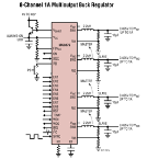
Eight-Channel Configurable 1A Buck DC/DCs for Multi-Rail Systems
The LTC3375 is a highly-integrated general-purpose power management solution for systems requiring multiple low voltage power supplies. The device features eight independent 1A channels with I²C control, flexible sequencing and fault monitoring in a compact QFN package. Each channel is a high efficiency synchronous step-down regulator with its own independent 2.25V to 5.5V input supply and an output voltage range of 0.425V to VIN. In addition, the LTC3375's buck DC/DCs may be connected in parallel to achieve higher output currents up to 4A per output with a single shared inductor. Up to four adjacent regulators can be combined, resulting in 15 different possible output configurations. All of the switching regulators are internally compensated and need only external feedback resistors to set the default output voltage. The LTC3375's pushbutton ON/OFF/RESET control, power-on reset and watchdog timer provide flexible and reliable power-up sequencing and system monitoring. All buck output voltages can be adjusted via I²C for margining or power optimisation. There is a die temperature monitor and an overtemperature warning function.This device features a programmable and synchronisable 1MHz to 3MHz oscillator with a 2MHz default switching frequency. It also contains a high voltage input shunt regulator controller, and quiescent current is only 11µA with all DC/DCs off. It is ideal for a wide variety of multichannel applications including industrial, automotive and communications systems.The LTC3375 is available in a thermally enhanced, low profile (0.75mm) 48-pin 7mm x 7mm exposed pad QFN package. E- and I-grades are specified over an operating junction temp range of -40°C to +125°C and the H-grade features operation from -40°C to +150°C. 1000-piece pricing starts at $5.45 each for the E-grade.Request a Quote Supplied by Analog Devices Ltd -
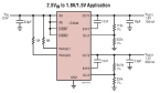
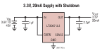
FMEA Compliant, 45V LDO Features 3µA IQ
The LT3007 is the latest member in a family of high voltage, micropower, robust PNP-based LDOs, featuring an ultralow 3µA quiescent current.
The LT3007's high input voltage capability, spanning 2.0V to 45V with an adjustable output voltage ranging from 0.6V to 44.5V, enables operation in a wide variety of application spaces.
This device's pinout is FMEA (Failure Mode Effects Analysis) compliant - the output stays at or below the regulation voltage during an adjacent pin short event, or if a pin is left floating.
The 3µA quiescent and shutdown (<1µA) currents enable ultralow standby power consumption, making the IC an excellent choice for applications not needing shutdown, or those requiring moderate output drive capability and high input voltage, such as remote monitoring and low-current battery-powered memory for "keep alive" systems that require extended run times.
The LT3007 delivers up to 20mA output current with a corresponding low dropout voltage of only 300mV. Output voltage tolerance is tightly regulated to within ±2% over line, load and temperature. The IC optimises stability and transient response with low ESR, ceramic output capacitors as small as 2.2µF. Internal protection circuitry includes reverse-battery protection, reverse output and reverse output-to-input protection, current limiting and thermal limiting for robustness.
The LT3007 is offered in both 'E' and 'I' grades in an 8-lead SOT-23 package with 3 pins fused to the ground paddle for enhanced thermal performance in both fixed and adjustable versions. 1,000-piece pricing starts at $1.20 each for the 'E' grade.
For more information, visit www.linear.com/product/LT3007.Request a Quote Supplied by Analog Devices Ltd -
FMEA Compliant, 45V LDO Features 3µA Quiescent Current
The LT3007 is the latest member in a family of high voltage, micropower, robust PNP-based LDOs, featuring an ultralow 3µA quiescent current.The LT3007's high input voltage capability, spanning 2.0V to 45V with an adjustable output voltage ranging from 0.6V to 44.5V, enables operation in a wide variety of application spaces.This device's pinout is FMEA (Failure Mode Effects Analysis) compliant - the output stays at or below the regulation voltage during an adjacent pin short event, or if a pin is left floating.The 3µA quiescent and shutdown (<1µA) currents enable ultralow standby power consumption, making the IC an excellent choice for applications not needing shutdown, or those requiring moderate output drive capability and high input voltage, such as remote monitoring and low-current battery-powered memory for "keep alive" systems that require extended run times.The LT3007 delivers up to 20mA output current with a corresponding low dropout voltage of only 300mV. Output voltage tolerance is tightly regulated to within ±2% over line, load and temperature. The IC optimizes stability and transient response with low ESR, ceramic output capacitors as small as 2.2µF. Internal protection circuitry includes reverse-battery protection, reverse output and reverse output-to-input protection, current limiting and thermal limiting for robustness.The LT3007 is offered in both 'E' and 'I' grades in an 8-lead SOT-23 package with 3 pins fused to the ground paddle for enhanced thermal performance in both fixed and adjustable versions. 1,000-piece pricing starts at $1.20 each for the 'E' grade.Request a Quote Supplied by Analog Devices Ltd -
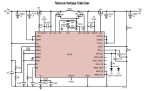
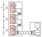
Guaranteed 0.04% Accurate Hybrid/Electric Battery Monitor Includes Isolated Interface
The LTC6804 is a high voltage battery monitor for hybrid electric and electric vehicles, and other high voltage, stacked-battery systems. An LTC6804 can measure up to 12 series connected battery cells at voltages up to 4.2V with 16-bit resolution and better than 0.04% accuracy. This high precision is maintained over time, temperature and operating conditions by a sub-surface Zener voltage reference similar to references used in precision instrumentation. When stacked in series the LTC6804 enables the measurement of every battery cell voltage in large high voltage systems. Six operating modes are available to optimize update rate, resolution and the low pass response of the built-in 3rd order noise filter. In the fastest mode all cells can be measured within 290µsec.Multiple LTC6804s can be interconnected over long distances and operated simultaneously, using Linear Technology's proprietary 2-wire isoSPI interface. Integrated into every LTC6804 the isoSPI interface provides high RF noise immunity up to 1Mbps and up to 100 meters of cable, using only twisted pair. Two communication options are available: with the LTC6804-1, multiple devices are connected in a daisy chain with one host processor connection for all devices; with the LTC6804-2, multiple devices are connected in parallel to the host processor with each device individually addressed.The LTC6804 has been engineered for ISO 26262 (ASIL) compliant systems and to surpass the environmental, reliability and safety demands of automotive and industrial applications with operation from -40°C to 125°C. Designed to minimize power consumption, especially during long-term storage where battery drain is unacceptable. In sleep mode it draws less than 4µA from the batteries. The LTC6804 is offered in a small 8mm x 12mm surface mount device priced at $10.95 each in 1,000-piece quantities.Request a Quote Supplied by Analog Devices Ltd -
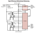
High Efficiency Bidirectional Multicell Active Balancer Maximizes Capacity Recovery in Series-Connected Battery Stacks
The LTC3300-1 is a high efficiency bidirectional multicell battery balancer for equalizing cell state of charge (SoC) in a series-connected battery stack. With the LTC3300-1 applications such as electric vehicles (EVs), plug-in hybrid EVs and large energy storage systems using cells with mismatched capacities are no longer limited by the lowest capacity cell in the stack. The LTC3300-1 goes beyond purely dissipative passive balancing solutions, enhancing battery performance by efficiently transferring charge to or from adjacent cells in order to bring mismatched cells into SoC balance within the stack. By redistributing charge throughout the stack, the LTC3300-1 compensates for lost capacity due to the weakest cells, enabling faster charging and extending the run time and usable lifetime of the battery stack.The LTC3300-1 is a key component in a high performance battery management system (BMS) for series-connected Li-Ion or LiFePO4 batteries. The device operates as a fault-protected controller IC for transformer-based bidirectional active balancing. The part utilises a non-isolated bidirectional synchronous flyback topology to balance up to 6 series-connected cells. Charge can be transferred between a selected cell and 12 or more adjacent cells. All balancers can operate independently and simultaneously with charge/discharge currents up to 10A. Bidirectional operation and simultaneous balancing minimizes the time required to equalize stack SoC, and the parts' high transfer efficiency (up to 92%) enables high current balancing with minimal power dissipation.The LTC3300-1 is offered in thermally enhanced surface-mount compatible packages: a low profile (0.75mm) 48-lead 7mm x 7mm QFN and a 48-pin 7mm x 7mm LQFP package. The 'I' grade is specified for both packages, with operating junction temperature range of -40°C to +125°C. 1,000-piece pricing starts at $5.95.Request a Quote Supplied by Analog Devices Ltd